In a sense electronic loads are the antithesis of power
supplies, i.e. they sink or absorb power while power supplies source power. In
another sense they are very similar in the way they regulate constant voltage
(CV) or constant current (CC). When used to load a DUT, which inevitably is
some form of power source, conventional practice is to use CC loading for devices
that are by nature voltage sources and conversely use CV loading for devices
that are by nature current sources. However most all electronic loads also feature
constant resistance (CR) operation as well. Many real-world loads are resistive
by nature and hence it is often useful to test power sources meant to drive such
devices with an electronic load operating in CR mode.
To understand how CC and CV modes work in an electronic
load it is useful to first review a previous posting I wrote here, entitled
“How Does a Power Supply Regulate It’s Output Voltage and Current?”. Again, the
CC and CV modes are very similar in operation for both a power supply and an
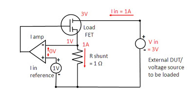
electronic load. An electronic load CC mode operation is depicted in Figure 1.
Figure 1: Electronic load circuit, constant current (CC)
operation
The load, operating in CC mode, is loading the output of
an external voltage source. The current amplifier is regulating the electronic
load’s input current by comparing the voltage on the current shunt against a
reference voltage, which in turn is regulating how hard to turn on the load FET.
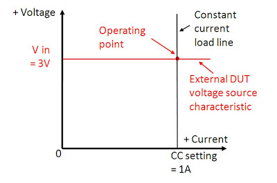
The corresponding I-V diagram for this CC mode operation is shown in Figure 2.
The operating point is where the output voltage characteristic of the DUT
voltage source characteristic intersects the input constant current load line
of the electronic load.
Figure 2: Electronic load I-V diagram, constant current
(CC) operation
CV mode is very similar to CC mode operation, as depicted
in Figure 3. However, instead of monitoring
the input current with a shunt voltage, a voltage control amplifier compares
the load’s input voltage, usually through a voltage divider, against a
reference voltage. When the input voltage signal reaches the reference voltage
value the voltage amplifier turns the load FET on as much as needed to clamp
the voltage to the set level.
Figure 3: Electronic load circuit, constant voltage (CV)
operation
A battery being charged is a real-world example of a CV
load, charged typically by a constant current source. The corresponding I-V
diagram for CV mode operation is depicted in figure 4.
Figure 4: Electronic load I-V diagram, constant voltage
(CV) operation
But how does an electronic load’s CR mode work? This
requires yet another configuration, as depicted in figure 5. While CC and CV modes
compare current and voltage against a reference value, in CR mode the control
amplifier compares the input voltage against the input current so that one is
the ratio of the other, now regulating the input at a constant resistance
value. With current sensing at 1 V/A and
voltage sensing at 0.2 V/V, the electronic load’s resulting input resistance value is 5 ohms for its CR mode
operation in Figure 5.
Figure 5: Electronic load circuit, constant resistance
(CR) operation
An electronic load’s CR mode is well suited for loading a
power source that is either a voltage or current source by nature. The
corresponding I-V diagram for this CR mode for loading a voltage source is
shown in Figure 6. Here the operating point is where the output voltage
characteristic of the DUT voltage source intersects the input constant
resistance characteristic of the load.
Figure 6: Electronic load I-V diagram, constant
resistance (CR) operation
As we have seen here an electronic load is very similar
in operation to a power supply in the way it regulates to maintain constant
voltage or constant current at its input.
However many real-world loads exhibit other characteristics, with
resistive being most prevalent. As a result most all electronic loads are
alternately able to regulate their input to maintain a constant resistance
value, in addition to constant voltage and constant current.


Hi I have a question: I have built the CV supply using this schematic and LM324 opamp and IRF3205 mosfet. I am testing a solar panel's I-V characteristics and I am not getting a smooth curve but a curve that dips violently after voltage starts increasing from zero. Then, the current comes back to an expected value and dips normally as I expect through the diode equation. Do you have any recommendations? Thank you!
ReplyDeleteHi Yunus,
ReplyDeleteFirst, these are conceptual circuit diagrams so you need to make certain that appropriate aspects are addressed to turn them into practical operating circuits; things like bias and operating level are correct for the range of operation, and frequency compensation for stable operation are addressed. Placing a capacitor across the lower leg of the resistive divider to create a dominant pole to roll off the frequency response many help. One area you may have some difficulty with testing a solar panel's I-V characteristic with a contant voltage load is at the zero/low current area, where the solar panel has more of a voltage characteristic as well. The difference in slope between the solar panel's and CV load's characteristics is small and it will be more difficult controlling the operating point. A constant resistance load may work better.
Regards, Ed
Thank you very much for your reply, Ed. I was wondering if you had some recommendations for an opamp feedback circuit. You see, I changed my opamp to an AD712 instead of the LM324 and the multisim simulations which were accurate for the LM324 (with the noisy curve) say that the circuit should absolutely work in this case, but I am getting at most 0.5V's at the output when I feed a 1A current source (sweeping the V-in reference doesn't change anything, unlike in the other case). In the previous case, the V- and V+ voltages were equalizing (which I don't see why as there is no obvious feedback circuit), but now they simply aren't. I know there are different types of opamps and is there one that you would recommend for this CV load?
ReplyDeleteI've been looking into how to best help you out here. I cannot say what op amps would be best; either of the two you bring up should be able to be made to work without too much trouble. There are too many unknowns for me to be able to recommend a feedback network. Ther are a couple of more things I can suggest however. First is to take note of how low of an operating voltage are you looking to achieve? Real low voltage operation may instead require adding a negative rail voltage to a design to maintain more voltage across the loading power element (FET) when operating at a low voltage. Another thing is the input capacitance of the FET. It is typically substantial to start with and increases quite a bit with low voltage operation. An op amp can run into stabilty issues when driving a capacitive load. You may also want to instead consider a BJT if the capacitance is a problem. Additional possiblities is to build a CV load using a TL431 and BJT configured as a shunt regulator or possibly use a linear audio amplifier IC of appropriate power rating as a CV load. Regards, Ed
ReplyDeleteI have 2 question
ReplyDelete1. How to make constant power mode CP ?
2. How to add in CR mode control signal from dac ?
Hi John,
ReplyDeleteTo make constant resistance programmable you would need to add a programmable gain amplifier stage (perhaps a voltage controlled amplifier controlled by a voltage out DAC) either after the current shunt voltage signal (which would cause the load resistance to increase) or after the voltage divider signal (which would cause the load resistance to decrease).
Constant power control would require even more circuitry to be added. Starting with the load circuit for constant resistance, the current shunt voltage signal and voltage divider voltage signal would both be fed into a multiplier circuit. The output of this multiplier would be voltage times current, or power. This would then need to be fed into the negative input comparison amplifier that controls the output. A voltage signal which would be the reference for the power level would then be fed into the positive input of the comparison amplifier. Regards, Ed
if it is possible to amplify .3 amps to 1 amps with constant voltage
ReplyDeleteHi Kiruthi,
ReplyDeleteFigures 3 and 4 show CV operation of an electronic load. I happened to use a DUT that is providing a constant current of 0.5 amps but this could be anything, including anywhere from 0.3 to 1 amp. What would be required is that the electronic load is capable of dissipating the maximum power and a practical electronic load design would include a current limit (like that shown in Figure 1) that would take control and limit the maximum amount of current that the electronic load is designed for, to protect it from over-current damage when operating as a CV load.