Showing posts with label Design. Show all posts

Tuesday, December 30, 2014

Why does an electronic load draw a pulse of current when a voltage is initially applied?

We recently had a customer contact us about one of our electronic loads. He had a solid state switch in series with a fixed output voltage source (for example, 50 V) and set the load to a fixed current (for example, 1 A). He used a current probe and a scope to observe the current flowing into the electronic load. When the switch changed from open to closed he saw a pulse of current flowing into the load that was significantly higher than the load set value before the load settled to the set value of 1 A. He was wondering if this was normal. It is normal. Here’s why:

The electronic loads have a snubber network across their input terminals. The snubber typically consists of a resistor in series with a capacitor. For example, the Keysight N3304A electronic load has 2.2 uF in series with about 2 ohms. The snubber network is there to maintain stability on the load input for all settings and operating modes. When the customer’s switch was closed, the initially discharged capacitor in the snubber pulled a pulse of current to begin charging. If the dV/dt of the load input voltage waveform was infinitely fast, the cap would initially look like a short and the initial current pulse would be limited by the resistor as I = V/R. In this example, the current pulse would have been 50 V / 2 ohms = 25 A. But he was seeing a much smaller current pulse: around 2.4 A instead of 25 A, but still higher than the expected set value of 1 A. This means the dV/dt was not infinite (the solid state switch had a finite risetime). In this case, the current pulse would be limited by the dV/dt of the input voltage waveform.

As an example, see Figure 1 below showing the input voltage and input current for an N3304A load. The voltage rises from 0 V to 50 V over about 75 us and the fastest part of the risetime is about 1V/us. Since I = C dV/dt, and for this electronic load, C = 2.2 uF, the peak of the current is calculated to be 2.2 uF x 1V/us = 2.2 A. The plot shows it to be about 2.4 A, so this is close to the expected peak value. As the dV/dt of the input voltage slows down, the current drops from its peak and approaches zero amps as the dV/dt slows to zero (horizontal). (Note that in the plot below, the load was set for zero current.)

So you can see that the current flowing into the input of an electronic load may not be simply the DC setting you expect. If you apply a dynamic voltage waveform to the input, the RC snubber network will also draw some current for a short time until the voltage applied to the load input stabilizes. There is another factor involved here that is worth mentioning but I will not cover in detail in this post since it is a secondary effect in this case. In this customer’s situation, the load was set for 1 A and initially had no voltage on it (his solid state switch was open). The load was trying to draw current by turning on its input FETs, but there was no voltage applied, so the load went to an unregulated state. When the voltage finally appeared (the solid state switch was closed), the FETs that were turned on hard had to recover and take a finite amount of time to begin regulating the set current. This effect can also contribute to brief, temporary unexpected current draw by the load when a voltage is suddenly applied to the input.

Saturday, November 29, 2014

Why do I measure voltage to earth ground on a power supply with a floating output?

Occasionally, one of our power supply users contacts us with a question about voltages measured from one of the power supply output terminals to earth ground (same as chassis ground). All of our power supply outputs are floating with respect to earth ground. See my previous post about this here. In that post, I stated that neither output terminal is connected to earth ground. To be more specific, no output terminal is connected directly to earth ground. We do have internal components, mainly resistors and capacitors, connected from each output terminal to earth ground. These components, especially the caps to ground, help mitigate issues with RFI (radio-frequency interference) and ESD (electrostatic discharge). They help prevent our power supplies from being susceptible to externally generated RFI and ESD, and also help to reduce or eliminate any internally generated RFI from being conducted to wires connected to the output terminals thereby reducing RFI emissions.

So even though our outputs are considered floating with respect to earth ground, there frequently is a DC path from at least one of our output terminals to earth ground. It is typically a very high value resistor, such as several megohms, but could be as low as 0.5 MΩ. This resistor acts as a bleed resistor to discharge any RFI or ESD caps to earth ground that could be charged to a high float voltage.

As an example of a power supply with a resistor to earth ground, the Keysight N6743A has 511 kΩ (~0.5 M) from the minus output terminal to earth ground. This resistor was responsible for the voltage measurements to earth ground observed and questioned by one of our power supply users. He was using this power supply in the configuration shown in Figure 1 and measured 9.7 Vdc from his common reference point to earth ground (again, same as chassis ground).


He understandably did not expect to measure any stable voltage between these points given that the output terminals are floating from earth ground. But once we explained the high impedance DC path from the minus output terminal to earth ground inside each power supply (see Figure 2), and the 10 MΩ input impedance of his DMM, the measurement made sense. The input impedance of the voltmeter (DMM) must be considered to accurately calculate the measured voltage. This is especially true when high impedance resistors are in the circuit to be measured.


Figure 3 shows the equivalent circuit which is just a resistor divider accounting for the 9.7 V measurement. (The exact calculation results in 9.751 V.) Notice that the voltage of the 28 V power supply does not impact this particular voltage measurement (but its resistor to ground does). If the user had measured the voltage from the plus output of the 28 V power supply to earth ground, both the 28 V supply and 20 V supply would have contributed to his measurement which calculates out to be 37.05 V (if you check this yourself, don’t forget to move the 10 MΩ resistor accounting for the different placement of the DMM impedance).


So you can see that even with power supply output terminals that are considered floating, there can still be a DC path to earth ground inside the supply that will cause you to measure voltages from the floating terminals to ground. As one of my colleagues always said, “There are no mysteries in electronics!”

Thursday, October 30, 2014

What is a reverse protection diode and what does it do?

A reverse protection diode is used on the output of a power supply to protect the power supply from damage due to an externally applied reverse voltage. Most power supplies have a polarized electrolytic capacitor (or several) across the output terminals. These caps help to filter ripple and noise on the output and provide a charge reservoir to reduce voltage sags and surges due to large load current changes. Electrolytic caps can withstand some reverse voltage, but not much. About 1 V to 1.5 V is the most they will tolerate without venting or worse…exploding! The reverse protection diode limits the reverse voltage to a diode drop thereby protecting the output caps. The diode is typically rated for the full output current of the power supply it is protecting. Adding to the diode drop, there can be some more small voltage drops due to current flowing in wires, tracks, current monitor resistors, output filter inductors, switching transformer windings, etc.

In a linearly regulated power supply, the reverse protection diode must be added to the design with the cathode connected to the plus output and anode connected to the minus output. See Figure 1. In a switching power supply, the reverse protection diode(s) is (are) an inherent part of the design. See Figure 2.


But where does reverse voltage come from? During normal operation, reverse voltage does not occur on the output of a power supply (unless it is a bipolar power supply which does not use polarized caps on its output…see this post). The power supply internal circuitry typically cannot produce reverse voltage on the output even if a failure occurs inside the power supply. So a reverse voltage has to be applied from an external source of power. For example, if you use two power supply outputs in parallel and inadvertently connect them to each other backwards, a reverse voltage would result. Another possibility can occur when two power supply outputs are connected in series. If the load across the series combination shorts, the two power supply outputs will be connected to each other backwards. See Figures 3 and 4. The reverse protection diode of one of the power supplies will conduct all available current from the other power supply forcing it into constant current (CC) operation and limiting the voltage to a diode drop (plus any additional small drops mentioned above).


So rest assured that your Keysight power supply is protected against reverse voltage if something unexpected happens!

Thursday, August 28, 2014

What can cause a power supply output voltage to exceed its setting?

We have done a number of posts on power supply protection topics covering both voltage and current issues:

Safeguarding your power-sensitive DUTs from an over power condition

How does power supply overvoltage protection work? 

Protect your DUT from over-current in more ways than one

What is a power supply’s over current protect (OCP) and how does it work?

Overvoltage protection: some background and history

Protect your DUT: use sense leads for overvoltage protection (OVP)

Types of current limits for over-current protection on DC power supplies

Protect your DUT with power supply features including a watchdog timer

And just last week, on August 20, 2014, my colleague and fellow Watt’s Up? blog contributor, Ed Brorein, presented a live webcast called “Protect Your Device Against Power-Related Damage During Test” which was recorded and can be accessed here. Before he presented the seminar, Ed mentioned it here.

Many of these posts talked about how the power supply responds to an overvoltage or overcurrent condition. Today I want to talk about what causes an overvoltage condition. I’m defining an overvoltage condition as a condition that causes the power supply output voltage to exceed its setting. Let’s take a look at some of the things that can cause this to happen.

Causes of power supply output voltage exceeding its setting

User-caused miswires
These miswires should be found and corrected during test setup verification before a device under test (DUT) is connected to the power supply. Possible miswires and their effect on the power supply output voltage are:

  • Shorted sense leads – the output voltage will rapidly rise above the setting. Keysight power supplies will prevent the output from rising above the overvoltage protection (OVP) setting.
  • Reversed sense leads – on most power supplies, the output voltage will rapidly rise above the setting and on Keysight supplies, it will be stopped by the OVP circuit. On our N6900/N7900 Advanced Power System (APS) power supplies, this condition is caught sooner: OV- is triggered when the output reaches about 10% of the rated voltage, so the output does not have to rise to the setting and above.
  • Open sense leads – If your power supply does not have protection for open sense leads, it is possible for your output to rapidly rise above the setting if one or both sense leads are open. Keysight power supplies have built-in sense protect resistors which limit the output voltage rise to about 1% above the setting. The voltage will continue to be regulated there. In addition to limiting the output to about 1% above the setting with an open sense lead, Keysight N6900/N7900 APS power supplies have a feature called open sense lead detection. When enabled, open sense lead detection will cause a sense fault (SF) status about 50 us after open sense leads are detected. This status does not turn off the output, but it can be configured to turn off the output using the advanced signal routing capability.
  • Special note about N7900 power supplies (not N6900): these models have output disconnect relays that open upon a protection fault. These mechanical relays take about 20 ms to open. Before they open, the output downprogrammer circuit is activated for about 2 ms and draws about 10% of rated output current to reduce the output voltage. The N7976A and N7977A (both higher voltage models) also have solid state relays in series with the mechanical relays. Upon a protection fault on these 2 models, the downprogrammer activates for 2 ms followed immediately by the solid state relays opening and then the mechanical relays open about 20 ms later.
Inadvertent wiring failure
  • Sense leads inadvertently become shorted – power supply response is the same as mentioned above under shorted sense leads
  • Sense leads inadvertently become open – power supply response is the same as mentioned above under open sense leads
  • Sense leads should never become inadvertently reversed, nevertheless, the power supply response is the same as mentioned above under reversed sense leads

Power supply fault (circuit failure)
Note that Keysight’s overall power supply failure rate is very low. Since the below mentioned failures are a subset of all failures, they are very rare. This means that failures that cause the output to go to a higher-than-desired value are a small percent of a small percent, and while not impossible, they are extremely unlikely events.
  • Power element fails (shorts)
    • Series regulator – when a series regulator power element shorts, the output very quickly rises above the rated voltage of the power supply. The only way to limit this is to trip OVP and either fire an SCR across the output to bring the voltage back down or open output relays. For example, the Keysight N678xA models use a series regulator. When OVP trips on N678xA models, output relays are opened to protect the DUT. Solid state relays very quickly open first followed by mechanical relays about 6 ms later.
    • Switching regulator – when a Keysight switching regulator power element shorts, the output will go toward zero volts instead of rising since Keysight switching regulators use power transformers and no power can be transferred through the transformer without the switching elements turning on and off. For example, all N6700 and N6900/N7900 series models use switching regulators except the N678xA models (series regulators).
    • Note that if a power element fails open using either power regulation scheme, the output voltage will fall, not rise, so this condition is not a concern when looking at excessive output voltage possibilities.
  • Regulation circuit failure (bias supply, DAC, amplifier, digital comparison processor, etc.)
    • There are various circuits that could fail and cause the output voltage to rise in an uncontrolled manner. Keysight power supplies have OVP designed to respond to these failures. In series regulators, an SCR across the output can fire to reduce the voltage or output relays can open. In switching regulators, the pulse width modulator is turned off to prevent power from flowing to the output, downprogrammers are activated to pull any excessive voltage down, and output relays are opened (when present) to disconnect the output from the DUT.
    • Multiple parallel failures – if both a regulating circuit fails that causes the output to rise AND the OVP circuit fails, there would be nothing to prevent the output voltage from rising above the setting. While this is possible, it requires just the right combination of multiple circuit failures and is therefore extremely unlikely.
Output response to load current transients
  • It is possible for the output voltage to temporarily rise above the setting for short transients in response to fast load current changes (especially unloading). If the voltage excursion is high enough and long enough, it is possible that the OVP will activate and respond as outlined above.

External power source
  • It is possible for an external source of power (such as a battery, charged capacitor, inductor with changing current, or another power supply) to cause the voltage to go above the setting. The OVP will respond to this condition as outlined above. If the external power source can provide more current than the rating of the power supply and an SCR circuit is used in the power supply, it is prudent to put a fuse in series with the external source of power to prevent damage to the power supply SCR and/or output circuit from excessive current.
So you can see that there are a number of ways in which the output voltage can rise above the setting. Luckily, Keysight design engineers are aware of these possibilities and have lots of experience adding protection circuits to prevent damage to your DUT!

Wednesday, July 30, 2014

How does power supply overvoltage protection work?

In past posts, I’ve written about what overvoltage protection (OVP) is (click here), where it is sensed (click here), and its history (click here). Today I want to cover a little about how it works inside the power supply.

As a quick review, OVP is a built-in power supply feature that protects the device under test (DUT) from excessive voltage by shutting down the power supply output if it senses voltage that exceeds the OVP setting. Depending on the power supply design, the voltage may be sensed at the output terminals or at the sense terminals.

Most of Agilent’s older power supplies sense OVP at the output terminals and use a simple analog comparator circuit to determine when the output exceeds the OVP threshold set by the user. The OVP threshold is translated into an overvoltage reference voltage (OVref) that could come from a simple divider with a potentiometer for adjustment (uncalibrated and rather crude) or from a more sophisticated calibrated digital-to-analog converter (DAC) voltage. When the comparator sees the scaled output voltage exceed the OVref voltage, the overvoltage trip (OVtrip) signal is generated which shuts down the power supply output and, on some designs, fires an SCR across the output. See Figure 1 for a simplified representation of this arrangement.

Some of our newer designs look for an overvoltage condition on the sense terminals for better accuracy. In this scheme, the sense voltage feeds one comparator input through a differential amplifier while the other comparator input is driven by the user-set calibrated OVref voltage. See Figure 2. An output terminal OVP as described above must also be used as a backup with these designs (not shown in Figure 2) because some OV conditions are not caught when sensing OV on the sense terminals. For example, if the sense leads are shorted together, the output voltage will go up uncontrolled yet the sense voltage will remain at zero volts.

Some other OVP designs use a calibrated analog-to-digital converter (ADC) on either the output terminal voltage or the sense terminal voltage and compare the measured digital data to the user’s threshold setting. See Figure 3. To avoid nuisance OVP shutdowns, this scheme frequently requires several analog-to-digital conversions in a row exceed the threshold (for example, 4). This adds a minor delay to the OVP response time. With fast ADC conversion rates, the OVP response can still be just a few tens of microseconds and it is worth spending a little extra time to gain immunity against nuisance tripping. For example, the Agilent N6781A uses this technique. Since it does an ADC conversion every 5 us and requires 4 consecutive conversions exceed the OVP threshold to cause a shutdown, it will trip in less than 30 us.

So you can see that there are various ways to implement overvoltage protection. In all cases, rest assured that your DUT is protected against excessive voltage when using Agilent power supplies!

Wednesday, November 13, 2013

How to Make More Accurate Current Measurements

There are a number of ways to make current measurements, including magnetically coupled probes, Hall-effect devices, and even some more exotic field sensing probes, but a good quality resistive shunt really cannot be beat in terms of accuracy, bandwidth, and overall general performance.

We likewise make considerable use of high performance shunts in our DC power products to provide extremely accurate current read-back of load currents, spanning the full range of output loading. Not only is the quality and design of the shunt itself critical, but how you treat it and make use of it are all equally important to get great current measurement performance. At the surface it may seem simple; it’s just measuring the voltage drop across a resistor. In reality it is no simple task. It requires appropriate metrological resources to validate the performance.  There are a lot of potential sources of error to recognize, quantify, and contend with.

When working with folks I sometimes encounter those who prefer to develop in their own current measurement into their test systems, instead of relying on the current read-back system already build into their system DC source. There are times when this is the right thing to do and is fine when done correctly. However some of the time there is the preconception that the DC source cannot provide an accurate measurement. The reality is there is a wide selection of DC sources available spanning a wide range of performance, Most likely something will be available that adequately addresses one’s needs. A second issue is, when developing current measurement capabilities for a test system, is truly recognizing all the potential sources of error. It goes well beyond having a good DVM and a good shunt resistor in the test system.  

A colleague here in our R&D group, Mark Peffley, wrote a comprehensive article that was just published. It covers a myriad of things in depth to be taken into consideration in order to make accurate current measurements, including:
  • Temperature dependencies
  • Self-heating and thermal equilibrium
  • Temperature gradients
  • Thermo-electric effects
  • Additional sources of offset errors
  • Voltage drop considerations
  • Shunt selection practical considerations
  • And more!
So using a shunt is a great foundation for making highly accurate current measurements. That’s why we use them in our power products. But, as Mark points out, there is a lot more to it than just Ohm’s law. When using one of our power products we factor all these things in so that they become a non-issue for the user. However, if you do plan to add current measurement into your test systems then I highly recommend reading Mark’s article “Obtain Accurate Current Measurement” (click here to access) as it is a great reference on the subject!

Friday, July 12, 2013

Why have multiple output range DC power supplies?

Most often DC power supplies have a rectangular output characteristic, as depicted in figure 1. With an increasing load they output a fixed output voltage up to the current limit, at which point the voltage drops in order to maintain the current fixed at its limit.


Figure 1: DC power supply rectangular output characteristic.

There is however DC power supplies that offer multiple output ranges. One example of a multiple (dual in this case) output range DC power supply is our N678xA series DC source measure modules. Their output characteristics are depicted in Figure 2.


Figure 2: Agilent N678xA series source measure modules output characteristics

Unlike the output characteristic of a single output range DC power supply, you cannot get both the maximum current and maximum voltage of a multiple output range DC power supply at the same time.

What is the purpose of having multiple output ranges on a DC power supply?
There are times, especially when having to test a variety of devices, the need for greater current or voltage, but not necessarily needing both maximum voltage and current at the same time.  In these situations many times these test power needs are better served by a DC power supply having multiple output ranges. The advantages of a multiple output range DC power supply are smaller size, less power dissipation, and less input power required, in comparison to a single output range DC power supply of comparable voltage and current capability. If the N678xA series DC source measure modules had a single output range they would need to have a 60 watt output to cover the span of voltage they now provide with 20 watts of output power.  An even more extreme example is our B2900 series source measure units. They output up to 31.8 watts continuously, but can provide up to 210 volts and up to 3.03 amps over three output ranges.

The downside of having multiple output ranges is somewhat greater complexity. Figure 3 depicts a conceptual design for a dual output range DC power supply. 


Figure 3: Conceptual dual output range DC power supply

Because the transformer efficiently converts AC power by square of its turn ratio there is very little impact on its size to accommodate secondary windings with multiple taps or multiple secondary windings that can be alternately connected in series or parallel, in order to accommodate multiple output power ranges. Similarly, the linear series pass element dissipates about the same maximum power whether it is operating at a higher voltage with lower current, or at a lower voltage with a higher current.  

The end result is a multiple range DC power supply can provide a greater range of voltages and currents for a given output power at the expense of a little greater complexity. Often this is far preferable to the alternative of a much higher power, and larger single output range DC power supply!

Monday, June 10, 2013

DC power supply output impedance characteristics

In a previous posting; “How Does a Power Supply regulate It’s Output Voltage and Current?” I showed how feedback loops are used to control a DC power supply’s output voltage and current.  Feedback is phenomenally helpful in providing a DC power supply with near-ideal performance. It is the reason why load regulation is measured in 100ths of a percent. A major reason for this is it bestows the power supply, if a voltage source, with near zero impedance, or as a current source, with high output impedance. How does it do this?

The impedance of a typical DC power supply’s output stage (like the conceptual one illustrated in the above referenced posting) is usually on the order of an ohm to a couple of ohms. This is the open-loop output impedance; i.e. the output impedance before any feedback is applied around the output.   If no feedback were applied we would not have anywhere near the load regulation we actually get. However, when the control amplifier provides negative feedback to correct for changes in output when a load is applied, the performance is transformed by the ratio of 1 + T, where T is loop gain of the feedback system. As an example, the output impedance of the DC power supply operating in constant voltage becomes:

Zout (closed loop) = Zout (open loop) / (1+T)

The loop gain T is approximately the gain of the operational amplifier times the attenuation of the voltage divider network. In practical feedback control systems the gain of the amplifier is quite large at and near DC, possibly as high as 90 dB of gain. This reduces the power supply’s DC and low frequency output to just milliohms or less, providing near ideal load regulation performance. Another factor in practical feedback control systems is the loop gain is rolled off in a controlled manner with increasing frequency in order to maintain stability. Thus at higher frequency the output impedance of a DC power supply operating as a voltage source increases towards its open loop impedance value as the loop gain decreases. This is illustrated in the output impedance plots in Figure 1, for the Agilent 6643A DC power supply.


Figure 1: Agilent 6643A 35V, 6A system DC power supply output impedance

As can be seen in Figure 1, for constant voltage operation, the 6643A DC power supply is just about 1 milliohm at 100 Hz, and exhibits an inductive output characteristic with increasing frequency as the loop gain decreases.

As also can be seen in Figure 1, feedback control works in a similar fashion for constant current operation. While a voltage source ideally has zero output impedance, a current source ideally has infinite impedance.  For constant current operation the 6643A DC power supply exhibits 10 ohms impedance at 100 Hz and rolls off in a capacitive fashion as frequency increases. However, for the 6643A, it is not so much the constant current control loop gain dropping off with frequency but the output filter capacitance dominating the output impedance. While the 6643A can be used as an excellent, well-regulated current source (see posting: “Can a standard DC power supply be used as current source?”) it is first and foremost optimized for being a voltage source. Some output capacitance serves towards that end.


An example of one use for the output impedance plots of a DC power supply is to estimate what the amount of load-induced AC ripple might be, based on the frequency and amplitude of the current being drawn by the load, when powered by power supply operating in constant voltage.

Wednesday, May 15, 2013

Power Factor and Active Power Factor Correction for Switched-mode Power Supplies


In my previous posting “More on Early Power Supply Preregulator Circuits” SCRs served to provide basically line frequency switched-mode operation for efficient power conversion and regulation in earlier mixed-topology DC power supply designs. Now that high frequency switched-mode power conversion circuits have long been highly refined, are physically much smaller, and are extremely cost effective they have become the game-changer. They can be used as a preregulator for mixed-topology DC power supply designs, as well as the complete DC power supply from the AC input to the regulated DC output, right? Well almost “yes”. They do bring all those of benefits over line frequency operation. As they can span a much wider range of AC input another benefit they bring is to eliminate the need for a complex AC line switch arrangement for the wide range of AC voltages needed.

It was recognized that one downside of high frequency switched-mode conversion is the AC input suffered from rather low power factor (PF). PF is the ratio of the real power to the apparent power. Low PFs cause increased losses in the AC power distribution system. Not only was it low, it was very non-linear, drawing current having high levels of odd harmonics. It turns out the third harmonic in particular can be additive, causing excessive current through the neutral line of AC power distribution systems. The reason for the low and non-linear PF is that the AC input of a high frequency switched-mode conversion circuit is a diode bridge feeding a large, high voltage, bulk storage capacitor, as shown in Figure 1. This non-linear load draws large peaks of current over short portions of the AC line period.


Figure 1: Non-linear AC load input of a high frequency switch-mode power converter circuit

As more and more electronic equipment was making use of switch-mode DC power supplies, minimum PF standards were established for products above a certain power rating, to avoid causing problems with the AC power distribution system. To meet the standards switch-mode DC power supplies above a certain power rating have had to incorporate power factor correction (PFC) into their AC inputs. While a few different approaches can be taken for adding PFC, most switch-mode DC power supplies incorporate a specialized switched-mode boost converter stage for providing active PFC. The active PFC stage is placed between the input rectifier bridge and bulk storage capacitor as depicted in Figure 2. An active PFC stage is designed to draw AC current in phase and in proportion to the AC voltage, typically providing PFs in a range of 0.95 to 0.99, which is comparable to a nearly purely resistive load!


Figure 2: Active PFC circuit in typical switched-mode DC power supply

While adding active PFC to a switch-mode DC power supply increases complexity, cost, and power loss somewhat, the overall combination of benefits of a switch-mode DC power supply with active PFC, either stand-alone or as a preregulator, is hard to beat!

Friday, May 10, 2013

More on Early Power Supply Preregulator Circuits


In my last posting “Ferroresonant Transformers as Preregulators in Early DC Power Supplies “, I introduced the concept of preregulators as a means of improving the efficiency of power supplies.  While a linear regulator provides excellent performance as a power supply, it has to dissipate all the additional power resulting from the voltage drop across it as it takes up the difference between the output voltage setting and the unregulated DC voltage at its input. This voltage difference becomes quite large for high-line AC input voltage levels, as well as low DC output voltage settings when the power supply has an adjustable output. A linear power supply becomes quite inefficient and physically large, having to dissipate a lot of power in comparison to what it provides at its output.  A preregulator helps to mitigate this disadvantage while still retaining the performance advantages of a linear output stage.

The ferroresonant transformer was a clever device and was an effective means of compensating for variance in the AC input voltage, but its output was fixed so it did not do anything for compensating for low DC output voltage settings when the power supply had an adjustable output.  A far more common type of preregulator circuit often used was an SCR preregulator circuit, depicted in Figure 1.


Figure 1: Constant voltage power supply with SCR preregulator

The SCR is a four layer diode structure. Unlike a conventional diode it does not conduct in the forward direction until a signal current is applied to its gate input. It then latches on and remains conducting in its forward direction. It does so until the forward bias voltage is removed or reversed and it resets. In the reverse direction it is the same as a conventional diode.  By replacing two of the conventional diodes in the full wave diode bridge with SCRs as shown in Figure 1, the DC voltage feeding into the linear regulator output stage can now be preregulated.  The preregulator control circuit senses the voltage across the series linear regulator output stage. For each half cycle of the line frequency it adjusts the firing angle of the SCRs in order to adjust the DC voltage at the input of the linear regulator so that the voltage across the linear regulator remains constant, compensating for the load and output voltage level setting accordingly. Figure 2 shows how changing the firing angle of the SCRs changes the output voltage and current delivered by the SCR preregulator circuit.


Figure 2: SCR firing angle control of the preregulator’s output

In all, an SCR preregulated power supply with a linear output stage provided a good balance of efficiency, performance, and cost making its topology well suited for DC power supplies for a variety of lab and industrial applications for the time.  Still, time marches on and high frequency switching-based topologies have come to dominate for the most part, due to a number of advantages they bring. As a matter of fact it is not uncommon today to find a switching power supply serving as a preregulator as well!


Reference: Agilent Technologies DC Power Supply Handbook, application note AN-90B, part number 5952-4020 “Click here to access”

Tuesday, April 23, 2013

Ferroresonant Transformers as Pre-regulators in DC Power Supplies


One significant drawback of a linear DC power supply is its efficiency for most applications. You can generally design a linear DC power supply with reasonable efficiency when both the output and input voltage values are fixed. However, when either or both of these vary over a wide range, after assuring the DC power supply will properly regulate at low input voltage and/or high output voltage, it then has to dissipate considerable power the other extremes.

For DC power supplies running off an AC line, having to accommodate a fairly wide range of AC input voltage is a given. A 35% increase in line voltage from the minimum to the maximum value is not uncommon. Today’s high frequency switching based power supplies have resolved the issue of efficiency as a function of input line voltage variance. However, prior to widespread adaptation of high frequency switching DC power supplies, variety of different types of low-frequency pre-regulators were developed for linear DC power supplies

What is a pre-regulator? A pre-regulator is a circuit that provides a regulated voltage to the linear output stage from an unregulated voltage derived from the AC line voltage, with little loss of power. Although not nearly as commonly used as other pre-regulator schemes, on rare occasion ferroresonant transformers were used as an effective and efficient pre-regulator in DC power supplies.

What is a ferroresonant transformer? It is similar to a regular transformer in that it transforms AC voltage through primary and secondary windings. Unlike a regular transformer however, once it reaches a certain AC input voltage level it starts regulating its AC output voltage at a fixed level even as the AC input voltage continues to rise, as depicted in Figure 1. Ferroresonant transformers are also commonly called constant voltage transformers, or CVTs.


Figure 1: Ferroresonant transformer input-output transfer characteristic

The ferroresonant transformer employs a rather unique magnetic structure that places a magnetic shunt leakage path between the primary and secondary windings. This structure is illustrated in Figure 2. This way only part of the transformer structure saturates at a higher fixed peak voltage level during each AC half cycle. When part of the core magnetically saturates, the primary and secondary windings are effectively decoupled. The AC capacitor on the secondary side resonates with existing inductance. This provides the carry-over energy to the load during this magnetically saturated phase, holding up the voltage level. The resulting waveform is a clipped sine wave with a fairly high level of harmonic distortion as a result. Some more modern designs include additional filtering that can bring the harmonic distortion down to just a few percent however.


Figure 2: Ferroresonant transformer structure

A ferroresonant transformer has some very appealing characteristics in addition to output voltage regulation:
  • Provides isolation from line spikes and noise that is normally coupled through on conventional transformers
  • Provides protection from AC line voltage surges
  • Provides carry over during momentary AC line drop outs that are of a fraction of a line cycle
  • Limits its output current if short-circuited
  • Extremely robust and reliable


Because of a number of other tradeoffs it is unlikely that you will find them in a DC power supply today. High frequency switching designs pretty much totally dominate in performance and cost. Ferroresonant transformer design tradeoffs include:
  • Large physical size
  • Relatively expensive and specialized
  • Limited to a specific line frequency as it resonates at that frequency


So, even though you are very unlikely to encounter a ferroresonant transformer in a DC power supply today, it’s interesting to see there still appears to be a healthy demand for ferroresonant transformers as AC line conditioners in a wide range of sizes, up to AC line power utility sizes.  Their inherent simplicity and robustness is hard to beat when long term, maintenance-free, reliable service is paramount, and AC line regulation in many regions around the world cannot be counted on to be well controlled.

Thursday, February 28, 2013

Overvoltage protection: some background and history

In my previous post, I talked about some of the differences between sensing an overvoltage condition on the output terminals of a power supply and sensing on the sense terminals. In this post, I want to cover some background and history about overvoltage protection (OVP).

OVP is a feature on a power supply that is used to prevent excessive voltage from being applied to sensitive devices that are being powered by the power supply. If the voltage at the output terminals exceeds the OVP setting, the output of the power supply shuts down, thereby protecting the device from excessive voltage. OVP is always active; you cannot turn it off. If you do not want it to activate, you should set it to a value that is much higher than the maximum voltage you expect at the output of your power supply.

An overvoltage condition can occur due to a variety of reasons:
·         Operator error - an operator can mistakenly set a voltage higher than desired
·         Internal circuit failure – an electronic circuit inside the power supply can fail causing the output voltage to rise to an undesired value
·         External power source – an external source of power, such as another power supply or battery in parallel with the output, could produce voltage that is higher than desired

Some power supply OVP designs include a silicon-controlled rectifier (SCR) across the output that would be quickly turned on if an overvoltage condition was detected. The SCR essentially puts a short circuit across the output to prevent the output voltage from going to a high value and staying there. The SCR circuit is sometimes called a “crowbar” circuit since it acts like taking a large piece of metal, such as a crowbar, and placing it across the power supply output terminals to protect the device under test (DUT) from excessive voltage.

Turning on an SCR across the output of a power supply as a response to an overvoltage condition originated as a result of older linear power supply designs. Linear regulators use a series pass transistor (click here for a post about linear regulators). If the series pass transistor fails shorted, all of the unregulated rail voltage inside the power supply appears across the output terminals. This voltage is higher than the maximum rated voltage of the power supply and can easily damage a DUT. When the OVP is activated, a signal is sent to turn off the series pass transistor. However, if that transistor failed shorted, the turn-off signal will be of no use. In this situation, the only way to protect the DUT is to trigger an SCR across the output to essentially short the output. Of course, the SCR circuit is designed to have a large enough capacity to handle the rail voltage and then the current that will flow when it is tripped. If a series pass transistor fails shorted, the AC input line fuse will sometimes blow when the SCR shorts which will completely disable the power supply protecting the DUT.

More recent power supply designs use switching regulation technology (click here for a post on switching regulators). Switching regulators have multiple power transistors that can fail. However, unlike the linear regulator design, when a switching transistor fails, it does not create a path between the rail voltage and the output terminals. So it is unlikely that a failed switching transistor will cause an OVP. And when an OVP activates for another reason in a switching regulator, all of the switching transistors are told to turn off, preventing any power from flowing to the output. As a result, there is no need for an SCR across the output for added protection against an overvoltage.

Decades ago, when OVP first started to be used on our power supplies (we were Hewlett-Packard back then), the OVP setting was fixed. It was internally set to maybe 10% or 20% above the maximum rated output of the power supply. Later, we provided the power supply user with the ability to crudely control the setting of the OVP by turning a potentiometer accessible through a hole in the front panel (see pictures below). The OVP range was typically adjustable from about 20% to 120% of the maximum rated output voltage of the power supply. When this feature first became available, it was offered as an add-on option for some power supply models. Later still, the front panel manually-adjustable OVP became standard on most high-performance power supplies. With advances in electronics, the OVP adjustability was moved deeper inside the supply and controlled with a DAC through front panel button presses or over an interface such as GPIB. Today, OVP is included in nearly every power supply, is set electronically, and is often a calibrated parameter to improve overall accuracy.

Friday, October 26, 2012

What is a bipolar (four-quadrant) power supply?

To answer this question, I have to start with a basic definition of polarity conventions. Figure 1 shows a simple diagram of a power supply (a two-terminal device) with the standard polarity for voltage and current. A standard power supply typically is a source of power. To source power, current must flow out of the positive voltage terminal. Most power supplies source energy in this way by providing a positive output voltage and positive output current. This is known as a uni-polar power supply because it provides voltage with only one polarity. By convention, the “polarity” nomenclature typically refers to the polarity of the voltage (not the direction of current flow).
If current flows into the positive voltage terminal, the power supply is sinking current and is acting like an electronic load – it is absorbing and dissipating power instead of sourcing power. Most power supplies do not do this although many Agilent power supplies can sink some current to quickly pull down their output voltage when needed – this is known as a down-programmer capability – see this post for more info: https://powersupplyblog.tm.agilent.com/2012/03/if-you-need-fast-rise-and-fall-times.html.

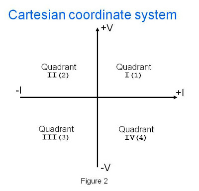
To fully define power supply output voltage and current conventions, a Cartesian coordinate system is used. The Cartesian coordinate system simply shows two parameters on perpendicular axes. See Figure 2.  By convention, the four quadrants of the coordinate system are defined as shown. Roman numerals are typically used to refer to the quadrants. For power supplies, voltage is normally shown on the vertical axis and current on the horizontal axis. This coordinate system is used to define the valid operating points for a given power supply. A graph of the boundary surrounding these valid operating points on the coordinate system is known as the power supply’s output characteristic.
As mentioned earlier, some power supplies are uni-polar (produce only a single polarity output voltage), but can source and sink current. These power supplies can operate in quadrants 1 and 2 and can therefore be called two-quadrant supplies. In quadrant 1, the power supply would be sourcing power with current flowing out of the more positive voltage terminal. In quadrant 2, the power supply would be consuming power (sinking current) with current flowing into the more positive voltage terminal.

Some power supplies can provide positive or negative voltages across their output terminals without having to switch the external wiring to the terminals. These supplies can typically operate in all four quadrants and are therefore known as four-quadrant power supplies. Another name for these is bipolar since they are able to produce either positive or negative voltage on their output terminals. In quadrants 1 and 3, a bipolar supply is sourcing power: current flows out of the more positive voltage terminal. In quadrants 2 and 4, a bipolar supply is consuming power: current flows into the more positive voltage terminal. See Figure 3.
Agilent’s N6784A is an example of a bipolar power supply. It can source or sink current and the output voltage across its output terminals can be set positive or negative. It is a 20 W Source/Measure Unit (SMU) with multiple output ranges. See Figure 4 for the output characteristic of the N6784A.
To summarize, a bipolar or four-quadrant power supply is a supply that can provide positive or negative output voltage, and can source or sink current. It can operate in any of the four quadrants of the voltage-current coordinate system.

Monday, October 15, 2012

Flyback Inverter for Fluorescent Lamp: Part 2, A Little Theory of Operation


In part 1 of this posting “Flyback Inverter for Fluorescent Lamp: Part 1, Making Repairs” a little careful and straightforward troubleshooting and repair brought my friend’s fluorescent lamp assembly back to life again. But a fluorescent lamp has quite a few unique requirements to get it to start up and stay illuminated. How does this flyback converter manage to do these things?

I had first looked around to see if I could find a schematic for this fluorescent lamp assembly, but nothing turned up for me. However, the parts count was low enough, and circuit board large enough, that it was a fairly simple matter to trace out and sketch the inverter’s schematic in fairly short order, as shown in Figure 1.


Figure 1: Fluorescent lamp single-ended flyback inverter circuit


When first powered up the switching transistor is biased on by the 812 ohm resistor, energizing transformer winding W1. This in turn applies positive feedback to the transistor through winding W2, driving it into saturation. There are two mechanisms in the flyback transformer that are critical for making this inverter work:
  • First it has a gapped core. This allows it to store a substantial amount of energy in its magnetic field which in turn gets dumped over to the fluorescent tube through the secondary winding W3 when the transistor turns off and the transformer’s magnetic field collapses.  During this period the winding voltage continues to climb as the magnetic field collapses until the energy can find a place to discharge to, in this case into the fluorescent tube. The voltage is also further increased by the turns ratio of the transformer. This is the “flyback” effect that creates sufficiently high enough voltage to get the fluorescent tube to “strike” or ionize its gas to get it to start conducting and give off illumination, typically many hundreds of volts.
  • As can be seen this inverter is a very simple circuit with a minimum of parts. A second mechanism in the transformer is it is designed to saturate in order to make the inverter oscillate. At the end of the transistor’s “on” period the transformer reaches its maximum magnetic flux at which point the transformer saturates. Winding voltage W2 drops to zero and then reverses driving the switching transistor into cutoff.  After the magnetic field has collapsed and energy discharged to the fluorescent tube the process repeats itself.


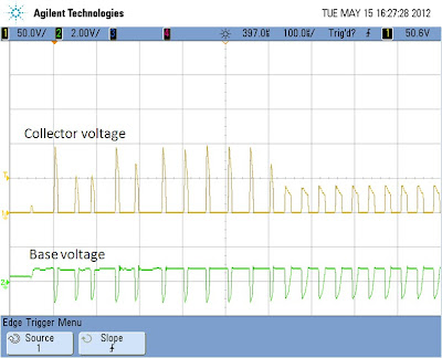
The switching transistor’s collector and base voltages during turn on are captured in the oscilloscope diagram shown in Figure 2.


Figure 2: Inverter switching transistor collector and base voltage waveforms

A number of interesting things can be observed in Figure 2.  The oscillation period is roughly 50 microseconds, or oscillation frequency of 20 kHz. It takes about 10 cycles, 500 microseconds, for the fluorescent tube to strike. During this initial phase the peak collector voltage is flying up to nearly 100 volts or about 8 times the DC input voltage being applied. Again, this voltage is being multiplied up by the turns ratio of windings W1 and W2 to bring this up in the vicinity of 600 volts or so needed to make the fluorescent tube to strike. Once the tube does strike and starts conducting its impedance drops. This causes the collector voltage to drop down to about 35 volts which is consistent with the proportion of drop in voltage needed for the fluorescent tube once it’s gas is ionized and is conducting. Note also the collector voltage pulse also widens as it takes a longer time for the energy in the transformer to be dumped when it’s at a lower voltage.

Although this inverter at first glance is a rather simple and minimum viable, minimum parts count circuit, with careful design it can be made to be very efficient. This is where the design of the transformer becomes as much art as science, knowing how the subtle characteristics of the magnetic material and inductive and capacitive parasitics can be used to advantage in contributing to and improving the overall performance of the design.

Anyway, what my friend really cared about is the lamp now works and he is able to put it to good use in his camper!

Thursday, October 4, 2012

Flyback Inverter for Fluorescent Lamp: Part 1, Making Repairs


A friend of mine approached me a while ago asking for some help. The fluorescent lamp assembly for his VW Westfalia camper was dead and, knowing I knew more about electronic devices than he did, figured it was worth challenging me with it.  I was actually happy to do so. Being involved with DC power conversion of a variety of forms I was always a bit curious to learn about how fluorescent lamp assemblies that were powered from low voltage DC worked anyway.

“My lamp does not work; can you look at it for me?”
“I suppose. Did it just stop working? Did you try anything to get it working again?”
“Well, it really never worked for me. I messed around with it a little but it did not help. I may have hooked it up backwards.”
“Why do you think you hooked it up backwards?”
“Well, it did not work so I tried reversing the power connections. That didn’t make it work however.”
“You really should not do that with electronic things!”

I took the lamp home and later when I had chance to look at it carefully I visually identified several problems. Like many other things I have repaired, a lot of the times it is not the device itself but rather a previous owner unintentionally inflicts unnecessary damage on it when attempting to make repairs.  In my friend’s partial defense, someone previously had already made unsuccessful attempts at trying to make it work again, unwittingly making things worse.

Referring to Figure 1 I unanchored the inverter circuit board from the back of the lamp assembly for closer inspection. It was immediately obvious there were problems that would keep it from working:
  • The connectors for the wiring to the fluorescent tube were not making contact.
  • A portion of a circuit board trace where the power feeds in was blown away.


Figure 1: Fluorescent lamp inverter board had obvious problems

Clearly someone had let the smoke out of it that made it work!  After making repairs to these problems I then tried powering it up using a power supply with a current limit to keep things safe. As I expected I was not going to get off that easy. The power supply went right up to its current limit setting. The lamp still did not work. 

The next step was to probe around the circuit board with a DMM.  With the abuse this lamp assembly has been subjected to I suspected the switching transistor would be damaged and sure enough it was measuring shorted. However, after removing it, it seemed to check out good. Probing around on the board again, a diode adjacent to the transistor measured shorted as well. Upon its removal it fell in half as a result of being overheated. I found where the rest of the smoke that makes it work had come out!  I replaced the diode, reinstalled the transistor and remounted the circuit board. Upon applying power again the result was a bit different as shown in Figure 2. I managed to reinstall all the smoke back into it again!


Figure 2: Fluorescent lamp assembly back in working order

While I had a general idea of how it works, now that I had the fluorescent lamp assembly working again I had take the opportunity to make some measurements and study the finer aspects of how it works, which I will cover, coming up in part 2. Stay tuned!

Wednesday, September 5, 2012

Early Power Transistor Evolution, Part 2, Silicon


As discussed in part 1 of this two-part posting on early power transistor evolution, by the early 1960’s germanium power transistors were in widespread use in DC power supplies, audio amplifiers, and other relatively low frequency power applications. Although fairly expensive at that time the manufacturers had processes establish to reliably produce them in volume. To learn more about early germanium power transistors click here to review part 1.

As with most all things manufacturers continued to investigate ways of making things better, faster, and cheaper. Transistors were still relatively new and ready for further innovation. Next to germanium silicon was the other semiconductor in widespread use and with new and different processes developed for transistor manufacturing, silicon quickly displaced germanium as the semiconductor of choice for power transistors. One real workhorse of a power transistor that has truly stood the “Test of Time” is the 2N3055, pictured in Figure 1. Also pictured is his smaller brother, the 2N3054.


Figure 1: 2N3055 and 2N3054 power transistors

Following are some key maximum ratings on the 2N3055 power transistor:
  • VCEO = 60V
  • VCBO = 100V
  • VEBO= 7V
  • IC = 15A
  • PD = 115W
  • hfe= 45 typical
  • fT = 1.5 MHz
  • Thermal resistance = 1.5 oC/W
  • TJ= 200 oC
  • Package: TO-3 (now TO-204AA)
  • Polarity: NPN
  • Material/process: Silicon diffused junction hometaxial-base structure


Diffused junction silicon transistors made major inroads in the early 1960’s ultimately making the germanium power transistors obsolete.  One huge improvement using silicon, especially for power transistors, is the junction temperature, which is generally rated for 200 oC.  This allowed operating at much higher ambient temperatures and at higher power levels when compared to germanium. 

While the alloy junction process being used for the early germanium transistors favored making PNP transistors, the diffused junction process on silicon favored making NPN transistors somewhat more. Silicon diffused junction NPN transistors are much more prevalent than PNP devices, and the PNP complements to NPN devices, where available, are more costly.  

The diffusion process made a giant leap in transistor mass production possible. Many transistors could now be made at once on a larger silicon wafer, greatly reducing the cost. The more precise nature of the diffusion junction over the alloy junction also improved performance. As one example, tor the 2N3055 the transition frequency increased roughly another order of magnitude over the 2N1532 germanium alloy junction transistor in part 1, to 1.5 MHz.  

The hometaxial-base structure is a single simultaneous diffusion into both sides of a homogenously-doped base wafer, one side forming the collector and the other side the emitter. A pattern on the emitter side is etched away around the emitter, down to the P-type layer, to form the base. The emitter is left standing as a plateau or “mesa” above the base.

The 2N3054 was electrically identical to the 2N3055 except for its lower current and power capabilities. It’s smaller TO-66 package however was never very popular and was quietly phase out in the early 1980’s, sometimes along with some of the devices that were packaged in it!

Process improvements beyond the single diffused hometaxial-base structure continued through the 1960s with silicon transistors, including double diffused, double- and triple diffused planar and epitaxial structures. The epitaxial structure is a departure from the diffused structures in that features are grown onto the top of the base wafer. With greater control of doping levels and gradients, and more precise and complex geometries, the performance silicon power transistors continued to improve in most all aspects.

Plastic-packaged power transistors have for the most part come to displace hermetic metal packages like the TO-3 (TO-204AA), first due to the lower cost of the part and second, with simpler mounting, reducing the cost and labor of the products they are incorporated into. One drawback of most of the plastic-packaged power devices is their maximum temperature rating has been reduced to typically 150 oC, taking back quite a bit of temperature headroom provided by the same devices in hermetic metal packages. Sometimes there is a price to be paid for progress! Pictured in figure 2 are two (of many) popular power device packages, the smaller TO-220AB and the larger TO-247.

Figure 2: TO-220AB and TO-247 power device plastic packages

It’s pretty fascinating to see how transistors and the various processes used to manufacture them evolved over time. In these two posts I’ve hardly scratched the surface of the world of power transistors and power devices. For one there is a variety of other transistor types not touched upon, including a variety of power FETs. Power FETs have made major inroads in all kinds of applications in power supplies. Also work continues to provide higher power devices in surface mount packages. These are just a couple of numerous examples, possibly something to write about at a future date!


References: “RCA Transistor Thyristor & Diode Manual” Technical Series SC-14, RCA Electronic Components, Harrison, NJ