Thursday, February 28, 2013

Overvoltage protection: some background and history

In my previous post, I talked about some of the differences between sensing an overvoltage condition on the output terminals of a power supply and sensing on the sense terminals. In this post, I want to cover some background and history about overvoltage protection (OVP).

OVP is a feature on a power supply that is used to prevent excessive voltage from being applied to sensitive devices that are being powered by the power supply. If the voltage at the output terminals exceeds the OVP setting, the output of the power supply shuts down, thereby protecting the device from excessive voltage. OVP is always active; you cannot turn it off. If you do not want it to activate, you should set it to a value that is much higher than the maximum voltage you expect at the output of your power supply.

An overvoltage condition can occur due to a variety of reasons:
·         Operator error - an operator can mistakenly set a voltage higher than desired
·         Internal circuit failure – an electronic circuit inside the power supply can fail causing the output voltage to rise to an undesired value
·         External power source – an external source of power, such as another power supply or battery in parallel with the output, could produce voltage that is higher than desired

Some power supply OVP designs include a silicon-controlled rectifier (SCR) across the output that would be quickly turned on if an overvoltage condition was detected. The SCR essentially puts a short circuit across the output to prevent the output voltage from going to a high value and staying there. The SCR circuit is sometimes called a “crowbar” circuit since it acts like taking a large piece of metal, such as a crowbar, and placing it across the power supply output terminals to protect the device under test (DUT) from excessive voltage.

Turning on an SCR across the output of a power supply as a response to an overvoltage condition originated as a result of older linear power supply designs. Linear regulators use a series pass transistor (click here for a post about linear regulators). If the series pass transistor fails shorted, all of the unregulated rail voltage inside the power supply appears across the output terminals. This voltage is higher than the maximum rated voltage of the power supply and can easily damage a DUT. When the OVP is activated, a signal is sent to turn off the series pass transistor. However, if that transistor failed shorted, the turn-off signal will be of no use. In this situation, the only way to protect the DUT is to trigger an SCR across the output to essentially short the output. Of course, the SCR circuit is designed to have a large enough capacity to handle the rail voltage and then the current that will flow when it is tripped. If a series pass transistor fails shorted, the AC input line fuse will sometimes blow when the SCR shorts which will completely disable the power supply protecting the DUT.

More recent power supply designs use switching regulation technology (click here for a post on switching regulators). Switching regulators have multiple power transistors that can fail. However, unlike the linear regulator design, when a switching transistor fails, it does not create a path between the rail voltage and the output terminals. So it is unlikely that a failed switching transistor will cause an OVP. And when an OVP activates for another reason in a switching regulator, all of the switching transistors are told to turn off, preventing any power from flowing to the output. As a result, there is no need for an SCR across the output for added protection against an overvoltage.

Decades ago, when OVP first started to be used on our power supplies (we were Hewlett-Packard back then), the OVP setting was fixed. It was internally set to maybe 10% or 20% above the maximum rated output of the power supply. Later, we provided the power supply user with the ability to crudely control the setting of the OVP by turning a potentiometer accessible through a hole in the front panel (see pictures below). The OVP range was typically adjustable from about 20% to 120% of the maximum rated output voltage of the power supply. When this feature first became available, it was offered as an add-on option for some power supply models. Later still, the front panel manually-adjustable OVP became standard on most high-performance power supplies. With advances in electronics, the OVP adjustability was moved deeper inside the supply and controlled with a DAC through front panel button presses or over an interface such as GPIB. Today, OVP is included in nearly every power supply, is set electronically, and is often a calibrated parameter to improve overall accuracy.

Protect your DUT: use sense leads for overvoltage protection (OVP)


Earlier this week, one of our military customers providing DC power to a very expensive device during test asked about the availability of a special option on one of our power supplies. He wanted the option that changed the location of the overvoltage protection (OVP) sensing terminals from the output terminals of the power supply to the sense terminals of the power supply. Since his device under test (DUT) is located quite a distance away from the power supply, he is using remote sensing to regulate the power supply voltage right at his device under test. (Click here for a post about remote sense.) And since the DUT is very expensive and sensitive to excessive voltage, he needs to protect the input of the DUT from excessive voltage as measured right at the DUT input terminals.

The power supply he is using, an Agilent N6752A installed in an N6700B mainframe, normally uses the output terminals as the sensing location for the overvoltage protection. (Click here for a post that includes a description of OVP.) OVP is used to prevent excessive voltage from being applied to sensitive devices. If the voltage at the output terminals exceeds the OVP setting, the output of the power supply shuts down. Since this customer is very interested in preventing excessive voltage from being applied to his expensive DUT, sensing for an overvoltage condition right at the DUT is important. For the N6752A, Agilent offers a special option (J01) that adds the ability to do OVP sensing with the sense leads. See Figure 1. With the J01 option added to his N6752A, the customer’s DUT is protected against excessive voltage.

You may be wondering why the standard OVP would sense at the output terminals instead of at the sense terminals. For decades, we have been making power supplies that sense OVP at the output terminals. Probably the biggest reason for sensing at the output terminals is because that approach provides more reliable protection than sensing at the sense leads even though it is less accurate. The output terminals are the power-producing terminals. If the sense leads become inadvertently shorted, the voltage at the output terminals would rise uncontrolled beyond the maximum rated output of the power supply. This uncontrolled high voltage could easily damage any device connected to the power supply’s output leads! So sensing for an overvoltage condition at the output terminals actually makes sense. It may not be the most accurate way to protect the DUT, but it is the most reliable given all of the things that can go wrong, such as a wiring error or an internal fault in the power supply.

The J01 option is available for only certain N67xx power modules. It adds the ability to sense for an overvoltage condition on the sense leads. This option does not remove the existing output terminal overvoltage sensing feature; it is in addition to it. Additionally, the J01 option is a tracking OVP option. You set a voltage value that is an offset from the programmed output voltage value. The J01 tracking overvoltage threshold tracks the real-time programming changes to the voltage setting and uses the remote sense leads to monitor the voltage.

Friday, February 15, 2013

Addressing the challenge of sequencing multiple bias supplies on and off


A challenge test engineers are perennially faced with is how to best sequence the bias voltages powering their DUT, when their DUT requires several bias voltages. Many DUTs are sensitive to sequencing and an improper sequence may lead to the DUT hanging up, or worse, suffer damage as a consequence. Not only is sequencing an issue when powering the DUT on, but it can also be an issue when powering the DUT down as well. In addition to sequencing, the slew rates of the various bias voltages can likewise be important to the DUT correctly powering on.

Simply relying on the timing of output-on and output-off commands sent from the test system controller to all the system DC power supplies individually tends to be far too imprecise, especially for critical sequencing timing requirements. The actual turn-on time of a typical system DC power supply can be many tens of milliseconds, and will vary considerably between different models of power supplies. The turn-on and turn-off times of each will need to be carefully characterized in order to know when a command for a specific bias voltage needs to be sent in relation to the other bias voltages. It is very likely the sequence of commands sent for outputs to turn on or off may be in a different sequence to the outputs actually changing, due to delay differences between different DC power supplies! An even bigger problem however is most system controllers are PCs which may randomly experience a large delay in sending out a command, if a higher level service request interrupts and pre-empts execution of the test program.

An alternative approach often taken is adding some custom hardware to control output sequencing. This can assure correct sequencing, but adds a lot of complexity, is usually inflexible, and may introduce other issues and compromises.

At Agilent we added system features to our N6700 series multiple output modular DC power system that support correct power-on and power-off sequencing. The output-on and output-off controls for the individual outputs get grouped together. The N6700 platform knows and compensates for the actual delays of all the various DC power output modules so that the desired delay value entered will be what is accurately achieved. Figure 1 shows setting up an N6705A to achieve a desired turn-on sequence of DC outputs for powering up a PC mother board. Figure 2 shows the actual result. A more detailed description of this PC motherboard example is given in our application note: “Biasing Multiple Input Voltage Devices in R&D”. While the N6705B DC Power Analyzer mainframe is regarded as being primarily for R&D, which this app note is referencing, the low profile rack-mountable N6700 series mainframes have these very same features and suit automated test systems in manufacturing and other environments.


Figure 1: Setting Output Delays


Figure 2: Output Turn-on Sequence Results


Just like setting up the power-on sequence, separate delays for power-off can also be entered, as seen in the set up screen shown in Figure 1, for the expected shut down of the DUT. However, what if there is an emergency shut down due to an abnormal condition and you still want to assure a certain power-off sequence? A colleague worked out the procedure for setting up the N6700 series DC power system to provide an orderly shutdown of the outputs, in the event of a problem on one of the outputs. In this example it happens to be an overvoltage condition on one of the outputs, but any of a number of fault conditions can be acted on to initiate an orderly shutdown. Details of this procedure are provided in another application note; “Avoid DUT Damage by Sequencing Multiple Power Inputs Off Upon a Fault Event”.

So when faced with the challenge of having to properly sequence multiple DC bias voltages powering your DUT, reconsider trying to engineer a solution to accomplish this. Instead, look for features that provide this kind of capability in the system DC power supplies you are looking to use, already built-in. It makes a lot of sense having sequencing built into the power supplies and it will make your life a lot easier!

Friday, February 8, 2013

Protecting your DUT using a power supply’s remote inhibit and fault indicator features


Paramount in most any good electronic test system is the need to adequately protect the device under test (DUT), as well as the test equipment, from inadvertent damage due to possible faults with the yet-untested DUT, accidental misconnections, misapplication of power, and a large number of other unanticipated events that can occur. It is no surprise that a lot of these unanticipated events by nature are related to the powering of the DUT. For this reason good system DC power supplies incorporate a number of features designed to protect both the DUT, as well as the power supply, in the event of an unanticipated fault occurring.  Two related protection features incorporated into our DC system power supplies are the remote inhibit and the discrete fault indicator (RI/DFI). These features provide real-time protection enabling immediate shutting down the power supply, as well as enabling the power supply to take immediate action, on the event of detecting the occurrence of an unanticipated event or fault.

The remote inhibit is a digital input control while the discrete fault indicator is a digital output control signal, incorporated into the digital I/O port on our system DC power supplies. An example of a digital I/O port is illustrated in Figure 1. When the digital I/O port is configured for fault/inhibit (also called RI/DFI) pins 1 and 2 are the open collector and emitter of an isolated transistor, to serve as a digital output control, and pin3 and 4 are the digital input and common for the inhibit control input. The remote inhibit and the fault indicator can be used independently as well as in combination, for protecting the DUT.


Figure 1: Multi-function digital I/O port on Agilent 6600A series system DC power supplies

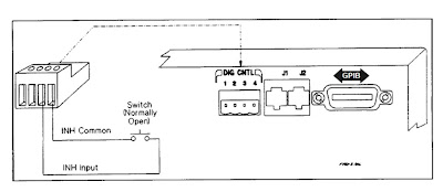
As the name implies, the remote inhibit is a digital control input, when activated, immediately disables the DC power supply’s output. One way this is commonly used is to connect an emergency shutdown switch that can be conveniently activated in the event of a problem. This may be a large pushbutton, or it may be a switch incorporated into a fixture safety cover. This arrangement is shown in Figure 2.


Figure 2: Remote inhibit using external switch

The fault indicator (i.e. FLT, FI, or DFI) digital output signal originates from the system DC power supply’s status system. The status system is a configurable logic system within the power supply having a number of registers that keep track of its status for operational, questionable, and standard events. Many of these events can be logically OR’ed together as needed to provide a fault output signal when particular, typically unanticipated, events occurs with the power supply. Items tracked by questionable status group register, like over voltage and over current, for example, are commonly selected and used for generating a fault output signal. An overview of the power supply status register system was discussed by a colleague in a previous posting. If you are interested in learning more; click here.
The fault indicator output can in turn be used to control an external activity for protecting the DUT, such as opening a disconnect relay to isolate the DUT, as one example, as depicted in Figure 3.


Figure 3: Fault output controlling an external disconnect relay

For DUTs that require multiple bias voltage inputs it is usually desirable that if a fault is detected on one bias input, that the other bias inputs are immediately shut down in conjunction with the one detecting a fault. The fault outputs and remote inhibit inputs on several DC power supplies can be used in combination by chaining them together, as depicted in Figure 4, to accomplish this task, to safeguard the DUT.


Figure 4: Chaining fault indicators and remote inhibits on multiple DC power supplies

The remote inhibit and fault indicator digital control signals on system DC power supplies provide a number of ways to disable power and take other actions for safeguarding the DUT. Their action is immediate, not requiring communication to, and intervention from, the test system controller. At the same time the system DC power supply generates status signals and can issue a service request (SRQ) to the test system controller so that it is notified of a problem condition and take appropriate correction action as well. The remote inhibit and fault indicator digital control signals are just two of many features found in many good system DC power supplies to assure the DUT is always adequately protected during test!