Saturday, February 28, 2015

Synchronize Your Measurements with Your List Transients

Hi everybody!

My blog post this month is the result of a recent customer question.  The question was: how do you synchronize measurements with list transients?  The short answer is that you use the built in digitizer to generate enough points to sample the measurements over the entire transient.  The rest of this blog will provide the long answer.  The program that I am using here was written for a N6762A DC Power Module but the technique will work with any power supply that has a built in digitizer such as the Advanced Power System or any N6700 module with option 054.

For simplicity’s sake, we are going to use a 5 point list.  The voltage steps are 1 V, 2 V, 3 V, 4 V, and 5 V and the dwell times are 0.1 s, 0.2 s, 0.3 s, 0.4 s, and 0.5 s.  Let’s first set the list up (please note that all programming is done in VB.net with VISA-COM):


The next thing to do is to set up the measurement system.  We need to figure out the total number of points that we need measure so that we can cover the entire transient.  The first thing that we need to do is to calculate the total time of the list transient (you can even do this in your program):


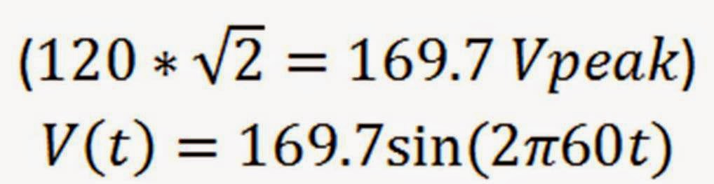
The total time of our transient is 1.5 s.  Now we need to use this to figure out the number of points. I am going to choose a measurement interval of 40.96 us.  This means that we want to take a measurement every 40.96 us for 15 s.  To get the total number of points, you need to divide the total transient time by the measurement time interval:

I’m going to round down and use 36,621 points.  I’m also going to tell the power supply to use the binary data format because as we know from my previous blog posts, this is the fastest way to read back data.   Here is the code to set up the digitizer:


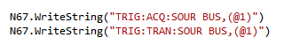
We will set our trigger source to bus for both the transient system and the acquire system:


Next we initiate both systems:


Once the initiate is complete, we send a trigger:

This will start both the list transient and the digitizer.  After everything is completed, we can fetch our measured voltage array:


This array will have all of our measurements.

I hope that this has been useful, have a good month everyone.


Thursday, February 26, 2015

When measurements and mathematics agree, I’m happy!

I have been an electrical engineer my entire career which will span 35 years in June (yikes….I’m too young to be this old!). Despite all of that time, plus the 4 years of undergraduate study before that and 3 years to get my MSEE at night while working full time during the day, I am still amused by some simple engineering principles. When the measurements I make in the real world completely agree with the hard-core theoretical mathematics I learned in school, I am amused.  Perhaps this should simply be expected (it is), but for some reason, I am still delighted when it happens. I recently had one of those simple experiences that I want to share with you today.

I was exploring some of the features on our new Keysight PA2201A IntegraVision power analyzer to better understand its operation and the applications for this new line of power measurement instrumentation. I had a simple desk lamp with a 100 W incandescent light bulb plugged into the wall outlet (120 Vac, 60 Hz here in the United States) and ran the voltage and current to the power analyzer. Given that the bulb presents a nearly pure resistive load to the sinusoidal voltage, as expected, the current was also a sine wave and in phase with the voltage. The power analyzer easily displays these measured waveforms.

What I never had an opportunity to see before was a visualization of the power waveform. For some reason, in all of my 35 years working in the power business, I never looked at a power waveform for a simple resistive load. Voltage? Sure! Current? Many times!! But power? Nope. The IntegraVision power analyzer shows voltage, current, and power waveforms as a typical display (this can be configured in quite a few other ways as well). So I was looking at the waveforms shown below.


The first thing I noticed about the power waveform was that it was sinusoidal and it never went below zero. This quickly made sense to me since I did consider the bulb to be purely resistive meaning it is consuming power 100% of the time, so all of the power flowing to the bulb had to be positive. The bulb is never pushing power back to the AC line as would happen with a reactive load especially for a purely reactive load such as a pure capacitor or inductor. If the load (the bulb) was not purely resistive, some of the power waveform would have dipped below the zero power line indicating that sometimes the load was absorbing power and sometimes it was providing power back to the line.

The next thing I noticed about the power waveform was that its phase was synchronized with the voltage and current, and it showed twice the frequency. Again, this quickly made sense since the power is simply the product of the voltage and the current [P(t) = V(t) * I(t)]. So the positive peaks have to line up (they do), the zero crossings of the voltage and current have to align with zero watts on the power waveform (they do), and the negative peaks in the voltage and current have to line up with another positive peak in the power since a negative voltage times a negative current yields a positive power (they do). This, of course, was the reason for the power waveform being twice the frequency of the voltage and current waveforms.

So I next decided to check the math behind the waveforms. I admit….I had to look up the trigonometric identity, but it was worth it! Since both the voltage and current waveforms are sine waves, and the power is the product of these, I looked up the identity for sine squared:
The voltage is a 120 Vrms, 60 Hz sine wave:
The current is 99.8 VA / Vrms = 0.832 Arms:
The power is V(t) * I(t):
Applying the above sine squared identity:
So you can see there is a 99.8 W fixed offset in the power waveform from which a cosine function is subtracted. The frequency of the cosine is 120 Hz (double the 60 Hz voltage and current waveforms). All of this completely agrees with the power waveform measured by the IntegraVision power analyzer. I am always thrilled when the math agrees with the measurements no matter how simple it is! How about you?

Tuesday, February 24, 2015

Two New Keysight Source Measure Units (SMUs) for Battery Powered Device and Functional Test

Over the past few years here on “Watt’s Up?” I have posted several articles and application pieces on performing battery drain analysis for optimizing run time on mobile wireless devices. The key product we provide for this application space is the N6781A 20V, +/-3A, 20W source measure module for battery drain analysis. A second related product we offer is the N6782A 20V, +/-3A, 20W source measure module for functional test. The N6782A has a few less key features used for battery drain analysis but is otherwise the same as the N6781A. As a result the N6782A is preferred product for testing many of the components used in mobile devices, where the extra battery drain analysis features are not needed. These products are pictured in Figure 1. While at first glance they may appear the same, one thing to note is the N6781A has an extra connector which is independent voltmeter input. This is used for performing a battery run-down test, one of a number of aspects of performing battery drain analysis. Details on these two SMUs can be found on by clicking on: N6781A product page.  N6782A product page,


Figure 1: Keysight N6781A SMU for battery drain analysis and N6782A for functional test

These products have greatly helped customers through their combination of very high performance specialized sourcing and measurement capabilities tailored for addressing the unique test challenges posed by mobile wireless devices and their components. However, things have continued to evolve (don’t they always!). Today’s mobile devices, like smart phones, tablets and phablets, have an amazing amount of capabilities to address all kinds of applications. However, their power consumption has grown considerably as a result. They are now utilizing much larger batteries to support this greater power consumption in order to maintain reasonably acceptable battery run-time. Optimizing battery life continues to be a critical need when developing these products. With their higher power however, there is in turn a greater need for higher power SMUs to power them during test and development. In response we have just added two new higher power SMUs to this family; the N6785A 20V, +/-8A, 80W source measure module for battery drain analysis and the N6785A 20V, +/-8A, 80W source measure module for functional test. These products are pictured in Figure 2. Details on these two new higher power SMUs can be found on by clicking on: N6785A product page.  N6786A product page.


Figure 2: Keysight N6785A SMU for battery drain analysis and N6786A for functional test

A press release went out about these two new SMUs yesterday; Click here to view. With their greater current and power capability, customers developing and producing these advanced mobile wireless devices and their components now have a way to test them to their fullest, not being encumbered by power limitations of lower power SMUs.

This is exciting to me having been working within the industry for quite some time now, helping customers increase battery life by improving how their devices make more efficient use of the battery’s energy. A key part of this has been by using our existing solutions for battery drain analysis to provide critical insights on how their devices are making use of the battery’s energy.  There is a lot of innovation in the industry to make mobile wireless devices operate with even greater efficiency at these higher power and current levels. There is no other choice if they are going to be successful. Likewise, it is great to see continuing to play a key role in this trend in making it a success!

.

Monday, February 9, 2015

Consider using an electronic load for generating fast, high-power current pulses

Often there is the need for generating high-power current pulses, typically of short duration, and having rise and fall times on the order of microseconds. This is a common need when testing many types of power semiconductors, for example.

When looking for a DC power supply capable of generating very fast, high-power current pulses, one will find there are not a lot of options readily available that are capable of addressing their needs. There are specialized products dedicated for specific applications like this; an example of this is Keysight’s B1505A purpose-built semiconductor test equipment. They are capable of generating extremely fast, high-power current pulses.

Apart from specialized products however, DC power supplies generally to not offer this kind of speed when operating in a constant current mode (or current priority mode). One exception that comes to mind that we provide is our N6782A and N6782A DC source measure modules. They can create fast current pulses having just a couple of microseconds of rise and fall time. However, they are limited to 20V, 3A, and 20W of output. Most of the higher power, more general-purpose DC sources are not able to generate these kinds of fast, high-power current pulses and most are really more optimized to operate as voltage sources.

One alternative to consider for generating fast, high-power current pulses when working with general-purpose test equipment is to use an electronic load. You may initially say to yourself “an electronic load is for drawing pulses of current, not sourcing them!” but when coupled to a standard DC power supply operating as a voltage source, the setup is able to source fast, high-power current pulses. Most electronic loads are designed to have very fast current response. To illustrate this, I helped one customer needing to test their high brightness LED (HBLED) arrays with fast pulses of current. This was accomplished with the setup shown in Figure 1.


Figure 1: Load setup generating fast, high power current pulses for LED array testing

In this setup the power supply operates as a fixed, static voltage source. The power supply’s output voltage is set to the combined total of the full voltage needed to drive the HBLED array at full current plus the minimum voltage needed for the electronic load. The minimum voltage required for the electronic load is when it conducting maximum current and most of the power supply voltage is then applied across the HBLED array. The electronic load’s required minimum voltage is that which supports its operation in its linear range and maintains full dynamic response characteristics. In the case of Keysight electronic loads this minimum voltage for linear dynamic operation is 3 volts.  Conversely the maximum voltage required for the electronic load is when it drops down to minimum current level, where the power supply’s voltage is instead now being dropped across the electronic load instead of the HBLED array. Note that the electronic load may need to maintain a very small amount of bleed current to maintain linear operation in order to provide truly fast rise and fall times. In this way the electronic load is able to regulate the current across the full range with excellent dynamic response. This can be seen in Figure 2 where we were able to achieve approximately 15 microsecond rise time right from the start.


Figure 2: Pulsed current rise time in HBLED array

One advantage of this setup is the wide range of voltage and power that can be furnished to the DUT using a relatively low power electronic load. A common characteristic of electronic loads is that they can dissipate a given amount of power over an extended range of current and voltage. When the electronic load is at maximum current it is at minimum voltage. Conversely when it is near or at zero current it is then at its maximum voltage. In both cases there is only a small amount of power that the electronic load needs to dissipate. For an HBLED array it does not conduct a lot of current until it reaches about 75% of its full operating voltage. As a result the electronic load does not see a lot of power even on a transient basis. For this particular situation we chose to use the Keysight N3303A 240V, 10A, 250W electronic load. This gave a wide range of voltage, current, and power for testing a comparably wide range of different HBLED array assemblies.

So next time you need to source fast, high-power current pulses, you may want to think “load” instead of “source”!


Friday, January 30, 2015

Using the Passthrough Command in IVI drivers

Hi everybody!

I was working on a customer question yesterday and I thought that it would make an enlightening blog post.  We have a feature for our IVI-COM and IVI-C drivers that allows you to directly send SCPI commands to your instrument.  This is really useful if you run into a situation where you think there is a function is missing from our driver or you run into something unexpected.  Overall, it is pretty easy to use once you know where to find it.

Let's look at the IVI-COM driver first.  You can find the passthrough in the Systems Interface under the IO property.  One you get to the IO level, you can just use the standard VISA-COM commands to send commands to the instrument and read responses back.  For my little example here I am just going to send a voltage measurement and read back the response:

In the code above, agDrvr is the name I gave to the instrument when I initialized it.

We also provide an IVI-C driver.  The IVI-C driver also has a passthrough command that is just a little more complicated than the IVI-COM version.. To send SCPI commands, you use the AgN67xx_SystemWrite function and to read data back you would use the AgN67xx_SystemRead function.  The same example as above would look like this:

In this IVI-C code:
status is where the IVI-C driver will report an error if there is an unsuccessful call 
session is the handle that I gave to this instrument when I initialized
32 was my best guess at the size of the response string.  I like to overestimate.
strResp is where I want the response to be stored
respSize is the actual size of the response and is returned by the program

All in all it's not too difficult and will definitely come in handy.  

That all I have for you this month.  As always, let us know if you have any questions.

Matt


Thursday, January 29, 2015

New Keysight Power Analyzer called IntegraVision

Back on June 23, 2014, I posted about the last Agilent power products to ever be announced. At that time, we had not yet officially changed our name from Agilent to Keysight. So the AC6800 AC sources we released on that date were released under the Agilent name, soon to be rebranded to Keysight. Well, today, I am announcing the first new Keysight power product: the Keysight Technologies IntegraVision Power Analyzer Model PA2201A.


A press release went out about these products earlier today: click here to view. We here at the Power & Energy Division of Keysight have been involved in power products for decades, and of course, Keysight has an oscilloscope division with commensurate experience producing scopes. I consider the new IntegraVision power analyzers to be a combination of the vast experience of our engineers from these two disciplines combining a power analyzer and an oscilloscope. The power analyzer will enable you to accurately measure parameters such as watts, VA, VAR, power factor, crest factor, efficiency, watt-hours, amp-hours, and harmonics while the oscilloscope will allow you to visualize in real time the voltage, current, and power waveforms that are important in your design.

I am very exciting about this new line of power measurement instruments! I have been working for HP/Agilent/Keysight for nearly 35 years now and have always worked with power products during my career. One of my favorite product families to support has been the older sophisticated 6800 AC Power Source/Analyzers (not to be confused with the newer basic AC6800 series mentioned in the first paragraph above). The older AC sources can produce sine waves, square waves, and arbitrary waveforms (for tests such as cycle dropout tests) as well as measure most of the power analyzer parameters mentioned above since they have a power analyzer built into the AC source. But now the new IntegraVision power analyzer goes well beyond the capabilities of the power measurements built into our AC sources. Adding time-based measurements like watt-hours and amp-hours opens up many more energy measurement application areas for this new product and the visual waveform measurements are a huge benefit when doing things like characterizing AC inrush current or product response to AC line disturbances. I am delighted with the performance of the touch-screen on this product – it will help you gain faster insight into your designs plus it just makes using the product fun! With 0.05% basic accuracy, 5 MSample/second 16-bit digitization, and inputs isolated to 1000 V, the IntegraVision power analyzer really is a superb product for power consumption and power conversion applications. Click here for the IntegraVision web page with links to the individual products.

So the next time you need a power analyzer with great accuracy and you also want to see the power waveforms related to your application, be sure to look at Keysight’s new IntegraVision Power Analyzer Model PA2201A. I’m sure you will not be disappointed! And look here for future posts about some of the interesting applications for this product, such as AC power line disturbance measurements and micro-inverter efficiency measurements. Suggest some of your own power measurements for me to make and I’ll see what I can do for a future post for you!

Wednesday, January 7, 2015

A new current measurement methodology: It’s all about counting the electrons going by!

One thing near and dear to us here at the Power and Energy Division is making accurate current measurements. What exactly is current? It’s basically the flow of electric charge per unit of time. In a conductor it’s the flow of electrons through it per unit of time. 

The ampere is the fundamental unit of current in coulombs per second, which equates to 6.241x10¹⁸ electrons per second. Accurate current measurement is one of the core values of virtually all of our products. Some of the precision SMU products can measure down to femtoamp (fA) levels (10-15 amps). This is where we tend to muse that we’re getting down to the levels where we’re virtually counting the individual electrons going by.

While there are a few different ways of measuring current, by far the most common is to measure the voltage drop across a resistive shunt. With careful design this provides the most accurate means of current measurement. There are a lot of non-obvious factors that can introduce unexpected errors that many are not aware of, leading them to believe they have better accuracy than what it really is. A good discussion of what it takes to truly make accurate current measurements was covered in a previous posting “How to make more accurate current measurements”(click here to review). We go through great pains in addressing these things in our products in order to provide accurate and repeatable measurements.

Unlike the volt and the ohm, which have quantum standards for their electrical units, the ampere instead relies on the standards for the volt and ohm for measurement, as a quantum standard for the ampere that directly relates it back to charge is still lacking. However, that may change in the not too distant future. A group of scientists were awarded the Helmholtz Prize in metrology for realization of the measurement of the ampere based on fundamental constants. Basically they’ve created an electron charge pump that moves a small, fixed quantity of electrons under control by a clock. You can say they’re literally “counting the electrons as they go by”. This could become the new SI standard reference for current measurement. To me this is very fascinating to find out about. More can be learned on this from the following link to the press release “Helmholtz Prize for the “new” ampere”(click here to review).  I am curious to see how this all plays out in the long run. Maybe it will lead to yet another, and better, way to make more accurate current measurements in products we all use today in our work in electronics!

Wednesday, December 31, 2014

Why is the Programming Resolution Supplemental Characteristic Listed as an Average?

Hello everyone!

Happy New Year!  This is our last post of 2014 so we wanted to wish all of our readers a Happy New Year.  Today I am going to talk about a question that I have been asked a few times lately.  In many of our power supplies, we list our Programming Resolution as an average number.  Many people want to know why we do it this way.

Look at the below snippet from our 664xA DC Power Supplies Supplemental Characteristics:


You can see that that it is clearly stated as an average.

The simple answer to this question is that this is because of calibration.

The more complex answer is that we use a DAC to control the output setting of the power supply.  A certain number of DAC counts is going to represent zero to full scale on the output of the supply.  For simplicity's sake, lets assume that we are using a 12 bit DAC for a power supply that goes to fifty volts.

In an ideal world where calibration is not necessary:
A 12 bit DAC gives us 2^12 or 4096 total counts.
The step size (programming resolution) of the 50 volt power supply would be 50/4096 or 0.0122 volts.

We do not live in an ideal world though so we have to disregard some DAC counts because of how the unit calibrates. We also generally let you program a little bit above the maximum settings (usually something like 2%).  Zero volts is not going to be zero DAC Counts and 50 V is not going to be 4096 DAC counts.  For our example, lets say that the minimum that we disregard 20 counts at the top and bottom (40 total counts) and the maximum we disregard is 120 counts (240 total counts) at the top and bottom.  In this scenario:

Minimum step size = 50/(4096-40) = 0.0123 V
Maximum step size = 50/(4096-120) = 0.0130 V

For our Supplemental Characteristic, we would take the average of those 2 numbers.   This gives us 0.01265 V.

The big question is how would I know what the programming resolution is for my particular unit.  I spent about half of yesterday trying to figure that out and I'm still working that out myself.  The best solution that I have right now is to hook a DMM to the output and slowly increment my output to see when it flips to a new setting.  I need to experiment on this though.  If any readers have a better idea, please let us know in the comments.  The fact of the matter is that the error is pretty small and to be safe, any error due to being in between DAC counts is included in our Programming Accuracy specification.

Well that is all for 2014. I hope that everyone has a safe and happy 2015.  See you next year!

Matt

Tuesday, December 30, 2014

Why does an electronic load draw a pulse of current when a voltage is initially applied?

We recently had a customer contact us about one of our electronic loads. He had a solid state switch in series with a fixed output voltage source (for example, 50 V) and set the load to a fixed current (for example, 1 A). He used a current probe and a scope to observe the current flowing into the electronic load. When the switch changed from open to closed he saw a pulse of current flowing into the load that was significantly higher than the load set value before the load settled to the set value of 1 A. He was wondering if this was normal. It is normal. Here’s why:

The electronic loads have a snubber network across their input terminals. The snubber typically consists of a resistor in series with a capacitor. For example, the Keysight N3304A electronic load has 2.2 uF in series with about 2 ohms. The snubber network is there to maintain stability on the load input for all settings and operating modes. When the customer’s switch was closed, the initially discharged capacitor in the snubber pulled a pulse of current to begin charging. If the dV/dt of the load input voltage waveform was infinitely fast, the cap would initially look like a short and the initial current pulse would be limited by the resistor as I = V/R. In this example, the current pulse would have been 50 V / 2 ohms = 25 A. But he was seeing a much smaller current pulse: around 2.4 A instead of 25 A, but still higher than the expected set value of 1 A. This means the dV/dt was not infinite (the solid state switch had a finite risetime). In this case, the current pulse would be limited by the dV/dt of the input voltage waveform.

As an example, see Figure 1 below showing the input voltage and input current for an N3304A load. The voltage rises from 0 V to 50 V over about 75 us and the fastest part of the risetime is about 1V/us. Since I = C dV/dt, and for this electronic load, C = 2.2 uF, the peak of the current is calculated to be 2.2 uF x 1V/us = 2.2 A. The plot shows it to be about 2.4 A, so this is close to the expected peak value. As the dV/dt of the input voltage slows down, the current drops from its peak and approaches zero amps as the dV/dt slows to zero (horizontal). (Note that in the plot below, the load was set for zero current.)

So you can see that the current flowing into the input of an electronic load may not be simply the DC setting you expect. If you apply a dynamic voltage waveform to the input, the RC snubber network will also draw some current for a short time until the voltage applied to the load input stabilizes. There is another factor involved here that is worth mentioning but I will not cover in detail in this post since it is a secondary effect in this case. In this customer’s situation, the load was set for 1 A and initially had no voltage on it (his solid state switch was open). The load was trying to draw current by turning on its input FETs, but there was no voltage applied, so the load went to an unregulated state. When the voltage finally appeared (the solid state switch was closed), the FETs that were turned on hard had to recover and take a finite amount of time to begin regulating the set current. This effect can also contribute to brief, temporary unexpected current draw by the load when a voltage is suddenly applied to the input.

Friday, December 12, 2014

Why Does Over Current Protect (OCP) have a Programmable Delay Value in the First Place?

Since I am on a roll about over current protect (OCP), having just completed a two-part posting “Why does the response time of OCP vary on the power supply I am using and what can I do about it?” (Review part 1) (Review part 2) there is yet another aspect about OCP that is worth bringing up at this time. And that is “why does OCP have a programmable delay value in the first place?” This actually came up in a discussion with a colleague here after having read my part posting.

It may seem a bit ironic that OCP has a programmable delay in that in my posting on OCP I shared ideas on how one can minimize the response time delay encountered. But this is not contradictory. One may very well want to minimize it, eliminating extra delay being encountered, but not necessarily eliminate it altogether. As can be seen in my previous postings, I had programmed the OCP delay time to 5 ms.

The programmable OCP delay does serve a purpose, and that is to prevent false OCP trips. Adding some delay time prevents these false trips.  For someone who knows the root cause of false OCP tripping they might be half right. There are actually been two main causes of false OCP trips which are prevented by adding some delay time.

The original problem with OCP was that it would be falsely tripped when output voltage settings were changed on the power supply, due to capacitive loading at the test fixture or within the DUT. This is especially prominent with inrush current when first bringing up the voltage to power the DUT. An OCP delay prevents false triggering under these conditions. To correct the false tripping the delay would be invoked when output programming changes were made. As one example, the OCP delay description in our manual for our 663x series power supplies states:

This command sets the time between the programming of an output change that produces a constant
current condition (CC) and the recording of that condition by the Operation Status Condition register. The
delay prevents the momentary changes in status that can occur during reprogramming from being
registered as events by the status subsystem. Since the constant current condition is used to trigger
overcurrent protection (OCP), this command also delays OCP.”

Under this situation the momentary overcurrent is induced by the power supply. Although not nearly as much as in issue in practice, momentary overcurrents can also be DUT-induced as well. This is the second situation that can cause a false tripping of the OCP. The DUT may be independently turned on after the bias voltage has already been on and draw a surge of current. Or the DUT may change mode of operation and draw a temporary surge of current.  If the OCP delay is invoked only by an output programming change it does not have any effect in these situations.

On later generation products, such as our N6700, N6900, and N7900 series, the user also has the ability to programmatically select between having the OCP delay activate from either an output change, or from going into CC condition. This gives the user a way to remain consistent with original operation or have OCP delay effective for momentary DUT-induced overload currents as well!


Friday, December 5, 2014

Why does the response time of OCP vary on the power supply I am using and what can I do about it? Part 2

In the first part of this posting (click here to review) I highlighted what kind of response time is important for effective over current protection of typical DUTs and what the actual response characteristic is for a typical over current protect (OCP) system in a test system DC power supply. For reference I am including the example of OCP response time from the first part again, shown in Figure 1.


Figure 1: Example OCP system response time vs. overdrive level

Here in Figure 1 the response time of the OCP system of a Keysight N7951A 20V, 50A power supply was characterized using the companion 14585A software. It compares response times of 6A and 12A loading when the current limit is set to 5A. Including the programmed OCP delay time of 5 milliseconds it was found that the actual total response time was 7 milliseconds for 12A loading and 113 milliseconds for 6A loading.  As can be seen, for reasons previously explained, the response time clearly depends on the amount of overdrive beyond the current limit setting.

As the time to cause over current damage depends on the amount of current in excess of what the DUT can tolerate, with greater current causing damage more quickly, the slower response at lower overloads is generally not an issue.  If however you are still looking how you might further improve on OCP response speed for more effective protection, there are some things that you can do.

The first thing that can be done is to avoid using a power supply that has a full output current rating that is far greater than what the DUT actually draws. In this way the overdrive from an overload will be a greater percentage of the full output current rating. This will normally cause the current limit circuit to respond more quickly.

A second thing that can be done is to evaluate different models of power supplies to determine how quickly their various current limit circuits and OCP systems respond in based on your desired needs for protecting your DUT. For various reasons different models of power supplies will have different response times. As previously discussed in my first part, the slow response at low levels of overdrive is determined by the response of the current limit circuit.

One more alternative that can provide exceptionally fast response time is to have an OCP system that operates independently of a current limit circuit, much like how an over voltage protect (OVP) system works. Here the output level is simply compared against the protect level and, once exceeded, the power supply output is shut down to provide near-instantaneous protection. The problem here is this is not available on virtually any DC power supplies and would normally require building custom hardware that senses the fault condition and locally disconnects the output of the power supply from the DUT. However, one instance where it is possible to provide this kind of near-instantaneous over current protection is through the programmable signal routing system (i.e. programmable trigger system) in the Keysight N6900A and N7900A Advanced Power System (APS) DC power supplies. Configuring this triggering is illustrated in Figure 2.


Figure 2: Configuring a fast-acting OCP for the N6900A/N7900A Advanced Power System

In Figure 2 the N7909A software utility was used to graphically configure and download a fast-acting OCP level trigger into an N7951A Advanced Power System. Although this trigger is software defined it runs locally within the N7951A’s firmware at hardware speeds. The N7909A SW utility also generates the SCPI command set which can be incorporated into a test program.


Figure 3: Example custom-configured OCP system response time vs. overdrive level

Figure 3 captures the performance of this custom-configured OCP system running within the N7951A. As the OCP threshold and overdrive levels are the same this can be directly compared to the performance shown in Figure 1, using the conventional, current limit based OCP within the N7951A. A 5 millisecond OCP delay was included, as before. However, unlike before, there is now virtually no extra delay due to a current limit control circuit as the custom-configured OCP system is totally independent of it. Also, unlike before, it can now be seen the same fast response is achieved regardless of having just a small amount or a large amount of overdrive.

Because OCP systems rely on being initiated from the current limit control circuit, the OCP response time also includes the current limit response time. For most all over current protection needs this is usually plenty adequate.  If a faster-responding OCP is called for minimizing the size of the power supply and evaluating the performance of the OCP is beneficial. However, an OCP that operates independently of the current limit will ultimately be far faster responding, such as that which can be achieved either with custom hardware or making use of a programmable signal routing and triggering system like that found in the Keysight N6900A and N7900A Advanced Power Systems.

Saturday, November 29, 2014

Why do I measure voltage to earth ground on a power supply with a floating output?

Occasionally, one of our power supply users contacts us with a question about voltages measured from one of the power supply output terminals to earth ground (same as chassis ground). All of our power supply outputs are floating with respect to earth ground. See my previous post about this here. In that post, I stated that neither output terminal is connected to earth ground. To be more specific, no output terminal is connected directly to earth ground. We do have internal components, mainly resistors and capacitors, connected from each output terminal to earth ground. These components, especially the caps to ground, help mitigate issues with RFI (radio-frequency interference) and ESD (electrostatic discharge). They help prevent our power supplies from being susceptible to externally generated RFI and ESD, and also help to reduce or eliminate any internally generated RFI from being conducted to wires connected to the output terminals thereby reducing RFI emissions.

So even though our outputs are considered floating with respect to earth ground, there frequently is a DC path from at least one of our output terminals to earth ground. It is typically a very high value resistor, such as several megohms, but could be as low as 0.5 MΩ. This resistor acts as a bleed resistor to discharge any RFI or ESD caps to earth ground that could be charged to a high float voltage.

As an example of a power supply with a resistor to earth ground, the Keysight N6743A has 511 kΩ (~0.5 M) from the minus output terminal to earth ground. This resistor was responsible for the voltage measurements to earth ground observed and questioned by one of our power supply users. He was using this power supply in the configuration shown in Figure 1 and measured 9.7 Vdc from his common reference point to earth ground (again, same as chassis ground).


He understandably did not expect to measure any stable voltage between these points given that the output terminals are floating from earth ground. But once we explained the high impedance DC path from the minus output terminal to earth ground inside each power supply (see Figure 2), and the 10 MΩ input impedance of his DMM, the measurement made sense. The input impedance of the voltmeter (DMM) must be considered to accurately calculate the measured voltage. This is especially true when high impedance resistors are in the circuit to be measured.


Figure 3 shows the equivalent circuit which is just a resistor divider accounting for the 9.7 V measurement. (The exact calculation results in 9.751 V.) Notice that the voltage of the 28 V power supply does not impact this particular voltage measurement (but its resistor to ground does). If the user had measured the voltage from the plus output of the 28 V power supply to earth ground, both the 28 V supply and 20 V supply would have contributed to his measurement which calculates out to be 37.05 V (if you check this yourself, don’t forget to move the 10 MΩ resistor accounting for the different placement of the DMM impedance).


So you can see that even with power supply output terminals that are considered floating, there can still be a DC path to earth ground inside the supply that will cause you to measure voltages from the floating terminals to ground. As one of my colleagues always said, “There are no mysteries in electronics!”

Monday, November 24, 2014

Prewired rack delivers up to 90 kW of single-output DC power

As I have mentioned before, I avoid posting product-only-focused material in this blog since our goal is to educate about power-related items rather than to directly promote Keysight products. But when something new comes out, I like to announcement it here.

A little over a year ago, Keysight (we were Agilent at the time) announced a new power supply family with high-power outputs up to 15 kW per output (see link here). These high-power autoranging DC power supplies with individual outputs up to 1500 V or 510 A can be paralleled for even more power. Paralleling outputs with these supplies is simplified since multiple outputs can be grouped to act as a single output and the current share bus enables multiple outputs to more equally share current. But there are other considerations when paralleling multiple units. Wiring the AC inputs and DC outputs together takes design time and assembly time. Integrating the units together physically in a rack also takes time and effort. Designing the system to ensure the safety of operators is also very important. So Keysight decided to offer a prewired rack to help you overcome the challenges associated with racking high-power supplies.

On November 11, 2014 (less than 2 weeks ago), we announced a prewired rack that combines up to six of the 15 kW N8900 series power supplies for total power up to 90 kW from a single output. You can choose from a variety of DC output combinations with voltages from 80 V to 1500 V and currents from 60 A to 3060 A. That’s a lot of current! The rack’s internal configuration makes the multiple outputs appear as a single output allowing you to communicate with just one power supply through LAN, GPIB, or USB (all standard in the system). Click here for the press release for this new system and here for additional system information.


Perhaps you are working in R&D or manufacturing on EV/HEV, alternative energy (fuel cells, solar, etc.), industrial DC motors, large UPS’s, electroplating, or any of the many other high-power application areas that need DC power up to 90 kW with voltages to 1500 V or currents to 3060 A. If so, and you want to spend your engineering resources on your core competencies instead of racking power supplies together, let Keysight help you with our new N8900 Series Rack System.

Tuesday, November 18, 2014

Why does the response time of OCP vary on the power supply I am using and what can I do about it? Part 1

In a previous posting of mine “Providing effective protection of your DUT against over voltage damage during test”(click here to review), an important consideration for effective protection was to factor in the response time of the over voltage protect (OVP) system. Due to the nature of over voltage damage, the OVP must be reasonably fast. The response time can typically be just a few tens of microseconds for a reasonably fast OVP system on a higher performance system power supply to hundreds of microseconds on a more basic performance system power supply. This response time usually does not vary greatly with the amount of over voltage being experienced.

Just as with voltage, system power supplies usually incorporate over current protect (OCP) systems as well. But unlike over voltage damage, which is almost instantaneous once that threshold is reached, over current takes more time to cause damage. It also varies in some proportion to the current level; lower currents taking a lot longer to cause damage. The I2t rating of an electrical fuse is one example that illustrates this effect.

Correspondingly, like OVP, power supply OCP systems also have a response time. And also like OVP, the test engineer needs to take this response time into consideration for effective protection of the DUT.  However, unlike OVP, the response time of an OCP system is quite a bit different. The response time of an OCP system is illustrated in Figure 1.


Figure 1: Example OCP system response time vs. overdrive level

Here in Figure 1 the response time of the OCP system of a Keysight N7951A 20V, 50A power supply was characterized using the companion 14585A software. It compares response times of 6A and 12A loading when the current limit is set to 5A. Including the programmed OCP delay time of 5 milliseconds it was found that the actual total response time was 7 milliseconds for 12A loading and 113 milliseconds for 6A loading.

This is quite different than the response time of an OVP system. Even if the OCP delay time was set to zero, the response is still on the order of milliseconds instead of microseconds for the OVP system. And when the amount of overdrive is small, as is the case for the 6A loading, providing just 1A of overdrive, the total response time is much greater. Why is that?

Unlike the OVP system, which operates totally independent of the voltage limit control system, the OCP system is triggered off the current limit control system. Thus the total response time includes the response time of the current limit as well. The behavior of a current limit is quite different than a simple “go/no go” threshold detector as well. A limit system, or circuit, needs to regulate the power supply’s output at a certain level, making it a feedback control system. Because of this stability of this system is important, both with crossing over from constant voltage operation as well as maintaining a stable output current after crossing over. This leads to the slower and overdrive dependent response characteristics that are typical of current limit systems.

So what can be done about the slower response of an OCP system? Well, early on in this posting I talked about the nature of over current damage. Generally over current damage is much slower by nature and the over drive dependent response time is in keeping with time dependent nature of over current damage. The important thing is understand what the OCP response characteristic is like and what amount of over current your DUT is able to sustain, and you should be able to make effective use of the over current protection capabilities of your system power supply.

If however you are still looking how you might further improve on OCP response speed, look for my follow up to this in my next posting!

Friday, November 7, 2014

Providing effective protection of your DUT against over voltage damage during test

The two most common ways DUTs can be electrically damaged during test are from current-related events or voltage-related events that mange to over-stress the DUT. Sometimes the cause can be an issue with the DUT itself. Other times it can be an issue stemming from the test system. The most common voltage-related damage to a DUT is an over voltage event, beyond a maximum level the DUT can safely tolerate. While there are a number of things that can cause this, most invariably it was an issue with the test system power supply, either from inadvertently being set too high or from an internal failure.

To protect against accidental over voltage damage, test system power supplies incorporate an over voltage protect (OVP) system that quickly shuts down the output upon detecting the voltage has gone above a preset threshold value. More details about OVP have been written about here in a previous posting “Overvoltage protection: some background and history”(click here to review).

The critical thing about over voltage damage is, in most all cases, that it is virtually immediate once the voltage threshold where damage to the DUT occurs is exceeded. It is therefore imperative that you optimize the test set up and settings in order to provide effective protection of your DUT against over voltage damage during test. To start with, the OVP trip threshold needs to be set at a reasonable amount below the threshold where DUT damage occurs and at the same time be set to a reasonable amount above the maximum expected DUT operating voltage. This is depicted in Figure 1.


Figure 1: OVP set point

However, to understand what are “reasonable amounts” above the maximum operating voltage and below the DUT damage voltage levels you need to take into account the dynamic response characteristics of the power supply output and OVP system, as depicted in Figure 2.


Figure 2: Power supply output and OVP dynamic response characteristics

It is important to have adequate margin above the maximum operating voltage to account for transient voltages due to the DUT drawing current from the power supply and resulting voltage response of the power supply in correcting for this loading, in order to prevent false OVP tripping. It is likewise important to adequate margin below the DUT damage threshold as it takes a small amount of time, in the range of 10’s to 100’s of microseconds, for the OVP system to start shutting down the power supply’s output once the OVP trip point has been crossed. At the same time the power supply typically has a maximum rate the output voltage can slew in. In practice these “reasonable amounts” typically need to be a few tenths to several tenths of a volt as a minimum.

Generally these margins are not difficult to manage, except when the DUT’s operating voltage is very small or the DUT operating current is very large producing a correspondingly large voltage drop in the power supply wiring. This is because the OVP is traditionally sensed on power supply’s output power terminals, so that it provides protection regardless of what the status and condition of the remote voltage sense wiring connection is. To improve on this we also provide OVP sensing on the remote sensing wires as an alternative to, or in addition to, the traditional sensing on the output power terminals. More details about this are described in another posting here “Protect your DUT: Use sense leads for over voltage protection (OVP)”(click here to review).

By following these suggestions you should be able to effectively protect your DUT against over voltage damage during test as well!

Friday, October 31, 2014

APS Paralleling Made Easier through Programming

Hi Everyone,

The Advanced Power Supply family has a very slick way to parallel units for higher current called current sharing.  This enables all of the paralleled units to be in Constant Voltage (CV) mode which is a change from most of our other power supplies that have one unit in CV mode and the rest of the units in Constant Current (CC) mode.  My colleague Ed did a very informative blog post about the different paralleling options that explains a bit more about paralleling units so I will not rehash any of that here.  Here is a link to that post: Paralleling Power Supplies.

The main drawback of the paralleling on the APS is that it can be a little difficult to get everything properly set to get the best performance.  You need to synchronize your current measurements and your voltage transients.  If you look in the manual, there are quite a few pages explaining how to set this all up.  I am happy to say that we have made this a little easier.  Our summer intern spent some time writing a VBA program in Excel that automatically does much of this.  The program uses Keysight VISA-COM so you need to have the Keysight IO Libraries installed to use it.  It will work with LAN, GPIB, and USB (all of which come standard on all APS units).

The first thing that we need to do is talk about the setup.  There are quite a few wire connections that need to be made.

First you need to connect the current sharing ports, the sense connections, and the outputs to the load:

After that, you also need to make some connections on the 8 pin  digital connector on the back of the APS units. You do not need to worry about setting up the pins if you plan on using the default pin assignments from the program.  The default pin assignments are:

Pin 6 on all units - On Couple
Pin 7 on all units - Off Couple
Pin 1 on the master unit - Trigger Out
Pin 1 on all other units - Trigger In
Pin 8 on all units - common

Here is a wiring diagram of the default assignments (for 3 units):


The On/Off Couple Pins make it so that when you enable or disable the output on any unit, all of the units enable or disable. The trigger line enable us to synchronize measurements as well as voltage changes.  

The Interface looks something like this:

It is divided into four boxes.  I will refer to them as boxes 1 to 4 with 1 being the left most box.  Box 1 is where you enter the VISA initialization string for each paralleled supply.  You can get this from the Keysight IO Libraries.  Box 2 is where you enter your settings  You can set the voltage limit, positive and negative current limit, change the output state, and change the voltage.  Most importantly, this is where you set the number of paralleled units.  This needs to be done or else the program will not work correctly.  You can parallel 1 kW and 2 kW units with each other, as long as they have the same maximum voltage so we also need to break out the number of 2 kW units in the scheme.  The third box will do a scalar measurement of the voltage and current.  This will report the total current of the paralleled units (it does a triggered measurement and adds all of the current measurements).  The fourth box will measure arrays of current and voltage (this function will not work on the N6900 APS units).      

I have posted this program on our Keysight Power Supply Forums at: Matt's Forum Post.  I have also opened a thread there where we can discuss this program.  It is still kind of preliminary so any feedback could possibly be incorporated into the program.  

That is all I have for this month.  Happy Halloween to all of our readers and please let me know any comments in the forum.


Thursday, October 30, 2014

What is a reverse protection diode and what does it do?

A reverse protection diode is used on the output of a power supply to protect the power supply from damage due to an externally applied reverse voltage. Most power supplies have a polarized electrolytic capacitor (or several) across the output terminals. These caps help to filter ripple and noise on the output and provide a charge reservoir to reduce voltage sags and surges due to large load current changes. Electrolytic caps can withstand some reverse voltage, but not much. About 1 V to 1.5 V is the most they will tolerate without venting or worse…exploding! The reverse protection diode limits the reverse voltage to a diode drop thereby protecting the output caps. The diode is typically rated for the full output current of the power supply it is protecting. Adding to the diode drop, there can be some more small voltage drops due to current flowing in wires, tracks, current monitor resistors, output filter inductors, switching transformer windings, etc.

In a linearly regulated power supply, the reverse protection diode must be added to the design with the cathode connected to the plus output and anode connected to the minus output. See Figure 1. In a switching power supply, the reverse protection diode(s) is (are) an inherent part of the design. See Figure 2.


But where does reverse voltage come from? During normal operation, reverse voltage does not occur on the output of a power supply (unless it is a bipolar power supply which does not use polarized caps on its output…see this post). The power supply internal circuitry typically cannot produce reverse voltage on the output even if a failure occurs inside the power supply. So a reverse voltage has to be applied from an external source of power. For example, if you use two power supply outputs in parallel and inadvertently connect them to each other backwards, a reverse voltage would result. Another possibility can occur when two power supply outputs are connected in series. If the load across the series combination shorts, the two power supply outputs will be connected to each other backwards. See Figures 3 and 4. The reverse protection diode of one of the power supplies will conduct all available current from the other power supply forcing it into constant current (CC) operation and limiting the voltage to a diode drop (plus any additional small drops mentioned above).


So rest assured that your Keysight power supply is protected against reverse voltage if something unexpected happens!

Wednesday, October 15, 2014

Creating a "bumping" auto-restarting over current protect on the N6900A/N7900A Advanced Power System

The two main features in system power supplies that have traditionally protected DUTs from too much current are the current limit and the over current protect (OCP). When a device, for any of a number of reasons, attempts to draw too much current, the current limit takes control of the power supply’s output, limiting the level of current to a safe level. An example of current limit taking control of a power supply output is shown in Figure 1.


Figure 1: Current limit protecting a DUT against excess current.

For those devices that cannot tolerate a sustained current at the current limit level, the over current protect can be set and activated to work with the current limit and shut down the power supply output after a specified delay time. This will protect a DUT against sustained current at the limit.  An example of an OCP shutting down a power supply output for greater protection against excess current is shown in Figure 2.


Figure 2: OCP protecting a DUT against excess current

We have talked about the current limit and OCP in previous posts. For more details on how the OCP works, it is worth reviewing “What is a power supply’s over current protect (OCP) and how does it work?” (Click here to review)

Sometimes it is desirable to have something that is in between the two extremes of current limit and OCP.  One middle-ground is a fold-back current limit, which cuts back on the current as the overload increases. More details about a fold-back current limit are described in a previous posting “Types of current limits for over-current protection on DC power supplies” (Click here to review). One thing about a fold-back current limit is the DUT and power supply will not be able to recover back into constant voltage (CV) operation unless the DUT is able to cut way back on its current demand.

Another type of current limit behavior that operates between regular current limit and OCP is one that shuts down the output, like OCP, but only temporarily. After a set period of time it will power up the output of the power supply again. If the DUT is still in overload, the power supply will shut down again. However, if the DUT’s overload condition has gone away, it will be able to restart under full power. In this way the DUT is protected against continuous current and at the same time it the power supply is not shut down and requiring intervention from an operator.

While this type of current limit is not normally a feature of a system DC power supply, it is possible to implement this functionality in the N6900A/N7900A Advanced Power System (APS) using its expression signal routing feature. This is a programmable logic system that is used to configure custom controls and triggers that run within the APS. Here the expression signal routing was used to create an auto-restarting current shutdown protect in the example shown in Figure 3.


Figure 3: Custom auto-restarting current shutdown protect configured for N6900A/N7900A APS

A custom control was created in the expression signal routing that triggers the output transient system to run if the current limit is exceeded for longer than 0.3 seconds. A list transient was programmed into the APS unit to have its output go to zero volts for 10 seconds and then return to the original voltage setting each time it is triggered. In this way the output would pulse back on for 0.3 seconds and then shut back down for another 10 seconds if the overload was not cleared. The custom trigger signal was graphically created and downloaded into the APS unit using the N7906A software utility, as shown in Figure 4.


Figure 4: Creating custom trigger for auto-restarting current shutdown protect on APS

Current limit and over current protect (OCP) are fairly standard in most all system DC power supplies for protecting your DUT against excess current. There are not a lot of other choices beyond this without resorting to custom hardware. One more option now available is to make use of programmable signal routing like that in the N6900A/N7900A APS. With a little ingenuity specialized controls like a auto-restarting current shutdown protect can be created through some simple programming.